X1241 – Preliminary Information
RWEL: Register Write Enable Latch—Volatile
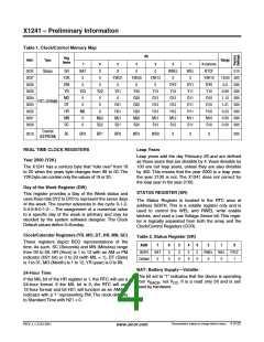
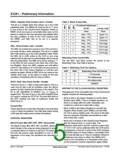
Table 3. Block Protect Bits
Protected Addresses
This bit is a volatile latch that powers up in the LOW
(disabled) state. The RWEL bit must be set to “1” prior
to any writes to the Clock/Control Registers. Writes to
RWEL bit do not cause a nonvolatile write cycle, so the
device is ready for the next operation immediately after
the stop condition. A write to the CCR requires both
the RWEL and WEL bits to be set in a specific
sequence.
X1241
Array Lock
None
0
0
0
0
1
1
1
1
0
0
1
1
0
0
1
1
0
1
0
1
0
1
0
1
None
600 - 7FF
Upper 1/4
Upper 1/2
Full Array
First Page
First 2 pgs
First 4 pgs
First 8 pgs
h
h
h
h
h
h
400 - 7FF
h
000 - 7FF
h
000 - 03F
h
WEL: Write Enable Latch—Volatile
000 - 07F
h
The WEL bit controls the access to the CCR and mem-
ory array during a write operation. This bit is a volatile
latch that powers up in the LOW (disabled) state. While
the WEL bit is LOW, writes to the CCR or any array
address will be ignored (no acknowledge will be issued
after the Data Byte). The WEL bit is set by writing a “1”
to the WEL bit and zeroes to the other bits of the Sta-
tus Register. Once set, WEL remains set until either
reset to 0 (by writing a “0” to the WEL bit and zeroes to
the other bits of the Status Register) or until the part
powers up again. Writes to WEL bit do not cause a non
volatile write cycle, so the device is ready for the next
operation immediately after the stop condition.
000 - 0FF
h
h
000 - 1FF
h
h
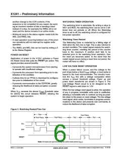
Watchdog Timer Control Bits
The bits WD1 and WD0 control the period of the
Watchdog Timer. See Table 4 options.
Table 4. Watchdog Time Out Options
WD1
WD0
Watchdog Time Out Period
1.75 seconds
0
0
1
1
0
1
0
1
750 milliseconds
250 milliseconds
disabled
RTCF: Real Time Clock Fail Bit—Volatile
This bit is set to a ‘1’ after a total power failure. This is a
read only bit that is set by hardware when the device
powers up after having lost all power to the device. The
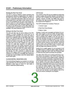
WRITING TO THE CLOCK/CONTROL REGISTERS
bit is set regardless of whether V
or V
is
Changing any of the nonvolatile bits of the clock/control
register requires the following steps:
CC
BACK
applied first. The loss of one or the other supplies does
not result in setting the RTCF bit. The first valid write to
the RTC (writing one byte is sufficient) resets the
RTCF bit to ‘0’.
– Write a 02H to the Status Register to set the Write
Enable Latch (WEL). This is a volatile operation, so
there is no delay after the write. (Operation pre-
ceeded by a start and ended with a stop).
Unused Bits
– Write a 06H to the Status Register to set both the
Register Write Enable Latch (RWEL) and the WEL
bit. This is also a volatile cycle. The zeros in the data
byte are required. (Operation preceeded by a start
and ended with a stop).
These devices do not use bits 3 through 6, but must have
a zero in these bit positions. The Data Byte output during
a SR read will contain zeros in these bit locations.
CONTROL REGISTERS
– Write one to 8 bytes to the Clock/Control Registers
with the desired clock, or control data. This
Block Protect Bits–BP2, BP1, BP0—Nonvolatile
sequence starts with a start bit, requires a slave byte
of “11011110” and an address within the CCR and is
terminated by a stop bit. A write to the CCR changes
EEPROM values so these initiate a nonvolatile write
cycle and will take up to 10ms to complete. Writes to
undefined areas have no effect. The RWEL bit is
reset by the completion of a nonvolatile write cycle,
so the sequence must be repeated to again initiate
The Block Protect Bits, BP2, BP1 and BP0, determine
which blocks of the array are write protected. A write to
a protected block of memory is ignored. The block pro-
tect bits will prevent write operations to one of eight
segments of the array. The partitions are described in
Table 3.
Characteristics subject to change without notice. 5 of 22
REV 1.1.3 2/13/01
www.xicor.com

 XICOR [ XICOR INC. ]