X1241 – Preliminary Information
another change to the CCR contents. If the
WATCHDOG TIMER OPERATION
sequence is not completed for any reason (by send-
ing an incorrect number of bits or sending a start
instead of a stop, for example) the RWEL bit is not
reset and the device remains in an active mode.
The watchdog timer is selectable. By writing a value to
WD1 and WD0, the watchdog timer can be set to 3 dif-
ferent time out periods or off. When the Watchdog
timer is set to off, the watchdog circuit is configured for
low power operation.
– Writing all zeros to the status register resets both the
WEL and RWEL bits.
Watchdog Timer Restart
– A read operation occurring between any of the previ-
ous operations will not interrupt the register write
operation.
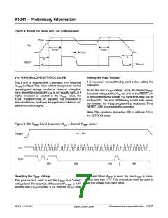
The Watchdog Timer is restarted by a falling edge of
SDA when the SCL line is high. This is also referred to
as start condition.The restart signal restarts the watch-
dog timer counter, resetting the period of the counter
back to the maximum. If another start fails to be
detected prior to the watchdog timer expiration, then
the reset pin becomes active. In the event that the
restart signal occurs during a reset time out period, the
restart will have no effect.
– The RWEL and WEL bits can be reset by writing a 0
to the Status Register.
POWER ON RESET
Application of power to the X1241 activates a Power
On Reset Circuit that pulls the RESET pin active. This
signal provides several benefits.
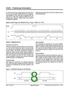
LOW VOLTAGE RESET OPERATION
– It prevents the system microprocessor from starting
to operate with insufficient voltage.
When a power failure occurs, and the voltage to the
part drops below a fixed V
voltage, a reset pulse is
– It prevents the processor from operating prior to sta-
bilization of the oscillator.
TRIP
issued to the host microcontroller. The circuitry moni-
tors the V line with a voltage comparator which
CC
– It allows time for an FPGA to download its configura-
tion prior to initialization of the circuit.
senses a preset threshold voltage. Power up and
power down waveforms are shown in Figure 4. The
Low Voltage Reset circuit is to be designed so the
RESET signal is valid down to 1.0V.
– It prevents communication to the EEPROM, greatly
reducing the likelihood of data corruption on power
up.
When the low voltage reset signal is active, the operation
of any in progress nonvolatile write cycle is unaffected,
allowing a nonvolatile write to continue as long as possi-
ble (down to the power on reset voltage). The low voltage
reset signal, when active, terminates in progress commu-
nications to the device and prevents new commands, to
reduce the likelihood of data corruption.
When V
exceeds the device V
threshold value
CC
TRIP
for 250ms the circuit releases RESET, allowing the
system to begin operation.
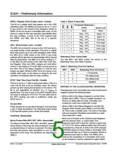
Figure 3. Watchdog Restart/Time Out
t
RSP
<t
t
>t
RSP WDO
t
t
>t
t
RST
t
RST
RSP WDO
RSP WDO
SCL
SDA
RESET
Note: All inputs are ignored during the active reset period (t
).
RST
Characteristics subject to change without notice. 6 of 22
REV 1.1.3 2/13/01
www.xicor.com

 XICOR [ XICOR INC. ]