Product Preview
WM8983
AUDIO SAMPLE RATES
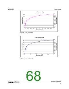
The WM8983 filter characteristics for the ADCs and the DACs are set using the SR register bits;
these bits do not change the rate of the audio interface output clocks in Master mode. The cut-offs
for the digital filters and the ALC attack/decay times stated are determined using these values and
assume a 256fs master clock rate.
If a sample rate is required which is not explicitly supported by the SR register settings, then the
closest SR value to that sample rate should be chosen, the filter characteristics and the ALC attack,
decay and hold times will scale appropriately.
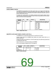
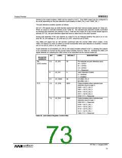
REGISTER
ADDRESS
BIT
LABEL
SR
DEFAULT
000
DESCRIPTION
R7
3:1
Approximate sample rate (configures the
coefficients for the internal digital filters):
Additional
Control
000 = 48kHz
001 = 32kHz
010 = 24kHz
011 = 16kHz
100 = 12kHz
101 = 8kHz
110-111 = reserved
Table 51 Sample Rate Control
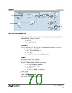
MASTER CLOCK AND PHASE LOCKED LOOP (PLL)
The WM8983 has an on-chip phase-locked loop (PLL) circuit that can be used to:
Generate master clocks for the WM8983 audio functions from another external clock, e.g. in
telecoms applications.
Generate and output (on pin CSB/GPIO1) a clock for another part of the system that is derived from
an existing audio master clock.
Figure 44 shows the PLL and internal clocking on the WM8983.
The PLL can be enabled or disabled by the PLLEN register bit.
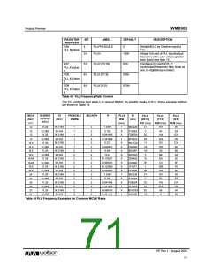
REGISTER
ADDRESS
BIT
LABEL
DEFAULT
DESCRIPTION
R1
5
PLLEN
0
PLL enable
0 = PLL off
1 = PLL on
Power
management 1
Table 52 PLLEN Control Bit
PP Rev 1.1 August 2005
69
w

 WOLFSON [ WOLFSON MICROELECTRONICS PLC ]