Product Preview
WM8983
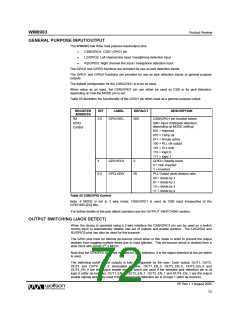
Similar to the output enables, VMID can be output to OUT3. This VMID output can be configured to
be on/off depending on the jack detection input polarity of VMID_EN_0 and VMID_EN_1.
The jack detection enables operate as follows:
All OUT_EN signals have an AND function performed with their normal enable signals (in Table 42).
When an output is normally enabled at per Table 42, the selected jack detection enable (controlled
by selected jack detection pin polarity) is set 0, it will turn the output off. If the normal enable signal is
already OFF (0), the jack detection signal will have no effect due to the AND function.
During jack detection if the user desires an output to be un-changed whether the jack is in or not,
both the JD_EN settings i.e. JD_EN0 and JD_EN1, should be set to 0000.
The VMID_EN signal has an OR function performed with the normal VMID driver enable. If the
VMID_EN signal is to have no effect to normal functionality when jack detection is enabled, it should
set to 0 for all JD_EN0 or JD_EN1 settings.
If jack detection is not enabled (JD_EN=0), the output enables default to all 1’s, allowing the outputs
to be controlled as normal via the normal output enables found in Table 42. Similarly the VMID_EN
signal defaults to 0 allowing the VMID driver to be controlled via the normal enable bit.
BIT
LABEL
DEFAULT
DESCRIPTION
REGISTER
ADDRESS
R9
GPIO control
5:4
JD_SEL
00
Pin selected as jack detection input
00 = GPIO1
01 = GPIO2
10 = GPIO3
11 = Reserved
6
JD_EN
0
Jack Detection Enable
0 = disabled
1 = enabled
8:7
3:0
JD_VMID
JD_EN0
00
[7] VMID_EN_0
[8] VMID_EN_1
R13
0000
Output enables when selected jack
detection input is logic 0.
0000 = OUT1_EN_0
0001 = OUT2_EN_0
0010 = OUT3_EN_0
0011 = OUT4_EN_0
0100-1111 = Reserved
7:4
JD_EN1
0000
Output enables when selected jack
detection input is logic 1
0000-0011 = Reserved
0100 = OUT1_EN_1
0101 = OUT2_EN_1
0110 = OUT3_EN_1
0111 = OUT4_EN_1
1000-1111 = Reserved
Table 56 Jack Detect Register Control Bits
PP Rev 1.1 August 2005
73
w

 WOLFSON [ WOLFSON MICROELECTRONICS PLC ]