WM8805
Production Data
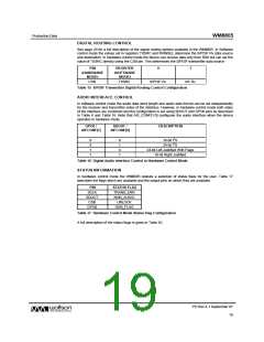
The oscillator uses a Pierce type oscillator drive circuit. This circuit requires an external crystal and
appropriate external loading capacitors. The oscillator circuit contains a bias generator within the
WM8805 and hence an external bias resistor is not required. Crystal frequencies between 10 and
14.4MHz or 16.28 and 27MHz can be used in software mode. The recommended circuit is shown in
the recommended components diagram, please refer to Figure 29.
Alternatively, an external CMOS compatible clock signal can be applied to the XIN pin in the absence
of a crystal, although this is not recommended when using the PLL as the PLL requires a jitter-free
OSCCLK signal for optimum performance.
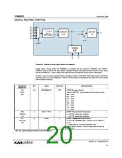
PHASE-LOCKED LOOP (PLL)
The WM8805 has an on-chip phase-locked loop (PLL) circuit that can be used to synthesise clock
signals from the external oscillator clock. The PLL can be used to:
•
Generate clocks necessary for the S/PDIF receiver to lock on to and recover S/PDIF data
from an incoming S/PDIF data stream.
•
•
Generate clocks which may be used to drive the MCLK and/or CLKOUT pins.
Generate clocks which may be used by the S/PDIF transmitter to encode and transmit a
S/PDIF data stream.
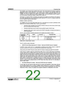
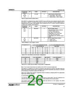
The PLL can be enabled or disabled using the PLLPD register bit as shown in Table 1.
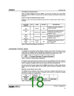
REGISTER
ADDRESS
BIT
LABEL
DEFAULT
DESCRIPTION
R30
PWRDN
1Eh
0
PLLPD
1
PLL Power Down Control
0 = Power up PLL
1 = Power down PLL
Table 20 PLL Power Down Control
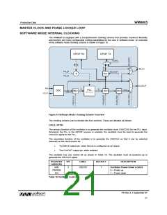
The PLL has two modes of operation:
•
S/PDIF Receive Mode (Automatic PLL Mode – Selected if S/PDIF Receiver Enabled)
In S/PDIF receive mode, the PLL is automatically controlled by the S/PDIF receiver to allow the
receiver to use the PLL to lock on to and track the incoming S/PDIF data stream.
Please refer to the S/PDIF Receiver section within the Internal Clocking description for full details.
If the CLKOUT or MCLK clocks are sourced from either CLK1 or CLK2 in this mode, the frequency
of these signals will be modified based on the clock rate of the incoming S/PDIF data stream. If the
sample rate of the incoming stream is changed, the MCLK and CLKOUT signals will continue to be
output, but will not be valid until the S/PDIF receiver has locked to the incoming stream at the new
sample rate. If the incoming S/PDIF stream stops, the PLL N and K values will be frozen and the
output clocks will continue at the frequency set by the last recovered S/PDIF stream. If the S/PDIF
input stream is removed then it is possible for the PLL to detect small pulse as the data is being
removed. This may result in the output clocks changing to an invalid frequency. Note also that if the
device is power-on and configured with no S/PDIF input data stream, then the PLL will default to
approximately 24MHz.
•
User Mode (Manual PLL Mode – Selected if S/PDIF Receiver Disabled)
In user mode, the user has full control over the PLL function and operation. In this mode, the user
can accurately specify the PLL N and K multiplier values (using the PLL_N and PLL_K registers),
divider values (PRESCALE and FREQMODE) and can hence control the generated CLK1 and CLK2
frequencies. Refer to Table 21 for details of the registers available for configuration in this mode.
PD Rev 4.1 September 07
22
w

 WOLFSON [ WOLFSON MICROELECTRONICS PLC ]