Production Data
WM8805
MASTER CLOCK AND PHASE LOCKED LOOP
SOFTWARE MODE INTERNAL CLOCKING
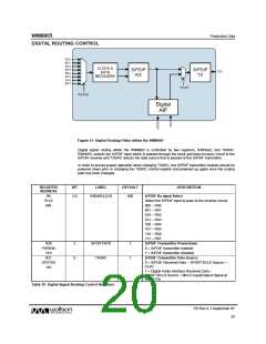
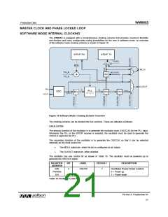
The WM8805 is equipped with a comprehensive clocking scheme that provides maximum flexibility
and function and many configurable routing possibilities for the user in software mode. An overview
of the software mode clocking scheme is shown in Figure 16.
Figure 16 Software Mode Clocking Scheme Overview
The clocking scheme can be divided into four sections. These are detailed as follows:
OSCILLATOR
The primary function of the oscillator is to generate the oscillator clock (OSCCLK) for the PLL input.
Whenever the PLL or the S/PDIF receiver is enabled, the oscillator must be used to generate the
OSCCLK signal for the PLL.
The secondary function of the oscillator is to generate the OSCCLK so that it can be selected
internally as the clock source for:
•
•
The MCLK output pin, when the pin is configured as an output.
The CLKOUT output pin, when enabled.
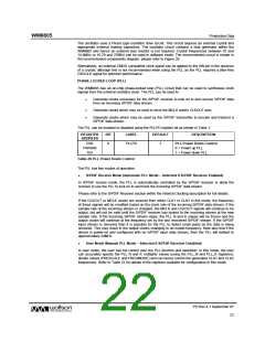
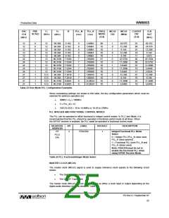
The oscillator has one control bit as shown in Table 19. The oscillator must be powered up to
generate the OSCCLK signal.
REGISTER
ADDRESS
BIT
LABEL
DEFAULT
DESCRIPTION
R30
PWRDN
1Eh
3
OSCPD
1
Oscillator Power Down Control
0 = Power up
1 = Power down
Table 19 Oscillator Control
PD Rev 4.1 September 07
21
w

 WOLFSON [ WOLFSON MICROELECTRONICS PLC ]