WM8805
Production Data
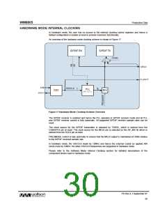
DESCRIPTION
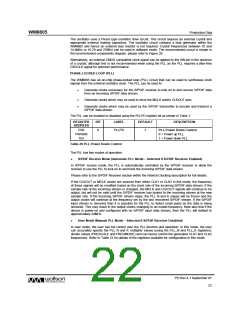
REGISTER
ADDRESS
BIT
LABEL
DEFAULT
R28
AIFRX
1Ch
6
AIF_MS
0
Audio Interface Mode Select
0 = Slave Mode – MCLK Input
1 = Master Mode – MCLK Output
Table 25 Audio Interface Mode Select
When MCLK is configured as an output, the MCLK source and rate can be selected using the control
bits shown in Table 26. The MCLK rate select can only be used when the MCLK output source is
selected as the PLL clock. If the oscillator clock is selected as the PLL source, the MCLK frequency
is equal to the oscillator clock frequency.
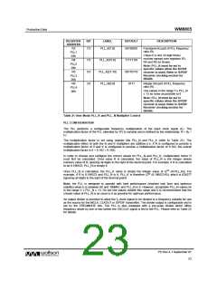
REGISTER
ADDRESS
BIT
LABEL
DEFAULT
DESCRIPTION
R7
PLL5
07h
3
MCLKDIV
0
MCLK Divider Select
(Only valid when CLK2 is selected
as MCLK output source)
See Table 27 for MCLKDIV
configuration in PLL user mode.
See Table 28 for MCLKDIV
configuration in PLL S/PDIF receive
mode.
R8
PLL6
08h
7
MCLKSRC
0
MCLK Output Source Select
0 = Select CLK2
1 = Select OSCCLK
Table 26 Master Clock Output Control
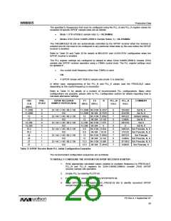
FREQMODE[1:0]
F2 TO CLK1 DIVISION FACTOR
CLKOUTDIV[1:0]
F2 TO CLK2 DIVISION FACTOR
MCLKDIV
00
÷2
÷2
÷4
÷6
01
÷2
10
÷4
11
÷8
0
÷2
÷4
÷8
÷12
1
00
01
10
11
÷4
÷4
÷8
÷16
÷32
÷48
÷8
÷8
÷16
÷24
÷16
÷24
÷12
Table 27 PLL User Mode Clock Divider Configuration
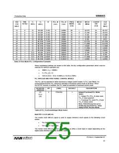
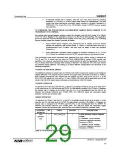
CLKOUTDIV[1:0]
CLK1 FREQUENCY
MCLKDIV
CLK2 FREQUENCY
00
01
10
11
512fs
256fs
128fs
64fs
0
1
256fs
128fs
Table 28 PLL S/PDIF Receive Mode Clock Divider Configuration
Note: The fs values shown above are relative to the S/PDIF recovered sample rate.
When MCLK is configured as an input, the reference clock rate for the S/PDIF transmitter (when the
digital audio interface received data is configured as the S/PDIF transmitter data source) is controlled
by the frequency of the MCLK signal at the MCLK pin.
Refer to the “Digital Audio Interface” datasheet section for details of configuring MCLK for appropriate
digital audio interface operation.
CLOCK OUTPUT (CLKOUT)
The high-drive clock output (CLKOUT) pin can be used as a clock output. This pin is intended to be
used as a clock source pin for providing the central clock reference for an audio system.
The CLKOUT clock source can be selected from either the OSCCLK or CLK1 signals. The control
bits for the CLKOUT signal are shown in Table 29.
PD Rev 4.1 September 07
26
w

 WOLFSON [ WOLFSON MICROELECTRONICS PLC ]