WM8805
Production Data
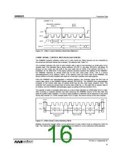
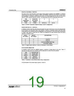
DIGITAL ROUTING CONTROL
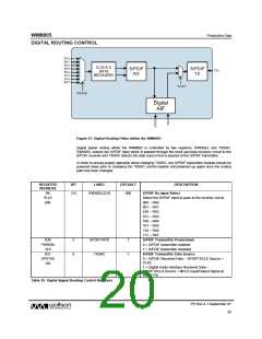
Figure 15 Digital Routing Paths within the WM8805
Digital signal routing within the WM8805 is controlled by two registers, RXINSEL and TXSRC.
RXINSEL selects the S/PDIF input which is passed through the clock and data recovery circuit to the
S/PDIF receiver and TXSRC selects the data source that is passed to the S/PDIF transmitter.
In order to ensure proper operation when changing TXSRC, the S/PDIF transmitter module should be
powered down prior to changing the TXSRC control register and powered up again once the routing
path has been changed.
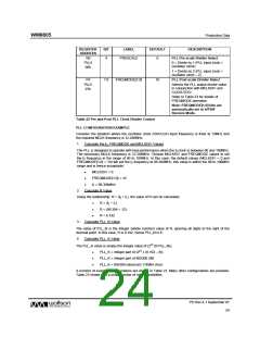
REGISTER
ADDRESS
BIT
LABEL
DEFAULT
DESCRIPTION
S/PDIF Rx Input Select
R8
PLL6
08h
2:0
RXINSEL[2:0]
000
Select the S/PDIF input to pass to the receiver circuit.
000 – RX0
001 – RX1
010 – RX2
011 – RX3
100 – RX4
101 – RX5
110 – RX6
111 – RX7
R30
PWRDN
1Eh
2
6
SPDIFTXPD
TXSRC
1
1
S/PDIF Transmitter Powerdown
0 = S/PDIF transmitter enabled
1 = S/PDIF transmitter disabled
S/PDIF Transmitter Data Source
R21
SPDTX4
15h
0 = S/PDIF Received Data – SPDIFTXCLK Source =
CLK2
1 = Digital Audio Interface Received Data –
SPDIFTXCLK Source = MCLK Input/Output Signal at
MCLK Pin
Table 18 Digital Signal Routing Control Registers
PD Rev 4.1 September 07
20
w

 WOLFSON [ WOLFSON MICROELECTRONICS PLC ]