WM8352
Production Data
happen before the I2C Acknowledge has been clocked by the host processor. If the /RST signal
causes the processor to reset before it has clocked the I2C Acknowledge, then the WM8352 will
continue to assert the Acknowledge signal (ie. pull the SDA pin low) after the processor has
completed its reset. On some processors, it may be necessary to toggle the SCLK pin in order to
clear the Acknowledge signal and resume I2C communications.
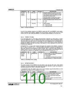
ADDRESS
BIT
LABEL
DEFAULT
DESCRIPTION
Allows the processors to reboot itself
0 = Do nothing
R3 (03h)
14
0
SYS_RST
System
Control 1
1 = Perform a processor reset by asserting
the /RST and /MEMRST (GPIO) pins for the
programmed duration
Protected by security key.
Table 61 Software Reset Command
14.4 DEVELOPMENT MODE
The WM8352 can start in different modes depending on the state of the CONF1 and CONF0 pins.
Development mode is selected by tying CONF1 and CONF0 to logic 0.
Development mode gives complete control over the configuration and startup behaviour of the
WM8352 and allows overriding the default values of selected registers (listed in Table 64). It enables
configuration of the WM8352 before startup. This is especially useful for evaluation and debugging.
In low-volume production, an external ‘genie’ (low-cost, small-size microcontroller) may be used to
configure the WM8352 in Development mode. The ‘genie’ is used to write the required register
values to generate the desired supplies and to configure the GPIO pins as required. These register
write operations can be achieved via a secondary control interface, which is provided by redirecting
the control interface to two GPIO pins as described below.
The configuration mode pins CONF1 and CONF0 should be tied to fixed logic levels. The start-up
sequence that they control is initiated on every transition from the OFF to the ACTIVE state.
14.4.1 CONTROL INTERFACE REDIRECTION
In Development mode, the 2-wire control interface is initially redirected from the primary control
interface (dedicated SDATA and SCLK pins, which require a DBVDD supply) to the secondary
control interface (the GPIO10 and GPIO11 pins, which can run on an externally generated supply
provided through the LINE pin). When using GPIO pins for the Control Interface, GPIO11 provides
the SDATA functionality, and GPIO10 provides the SCLK functionality.
Use of the secondary interface makes it possible to configure the WM8352 before the DBVDD supply
voltage becomes available (e.g. in the OFF and PRE-ACTIVE states). The control interface can be
switched back to the primary interface at any time by writing to the USE_DEV_PINS bit. In a typical
application, the primary control interface would be selected after the WM8352 is fully configured.
The device address for the secondary control interface is 0x34h, and cannot be changed. In
development mode only, the primary interface address can be selected by writing to the DEV_ADDR
bits through the secondary interface. Note that this functionality is only available in Development
mode.
PD, February 2011, Rev 4.4
112
w

 WOLFSON [ WOLFSON MICROELECTRONICS PLC ]