Production Data
WM8352
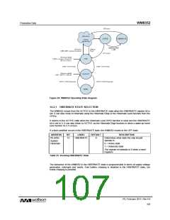
14.3.6 RESET SIGNALS
The WM8352 provides an active-low reset output signal to the host processor on the open-drain
/RST pin. The /RST pin is asserted low in the OFF state. The status of the /RST pin in HIBERNATE
state is configurable using the RST_HIB_MODE bit.
In start-up, after all enabled power supplies reach 90% of their programmed output voltage, the /RST
output is held low for a programmable duration set by RSTB_TO. The /RST pin is then set high. The
/RST output is set low during the shutdown sequence.
In Configuration Mode 10 only, the “crystal detect” mode is enabled; this controls the /RST output
behaviour. In this mode, the WM8352 monitors the 32kHz crystal oscillator during start-up to verify
that the output frequency is valid. The /RST output is held low until this has been achieved.
An additional GPIO output, /RST can be generated, with the same functionality as the /RST pin. A
GPIO pin must be configured as /RST in order to output this signal (see Section 20).
The WM8352 can also generate a separate /MEMRST signal for other subsystems such as external
memory. This allows resetting some subsystems in the HIBERNATE state, while not resetting others.
The /MEMRST feature is provided via a GPIO pin (see Section 20). Note that /MEMRST is not a
valid control signal during the start-up as the GPIO pins are not configured at this time. The
MEM_VALID field provides an indication of whether the contents of the external memory (under
control of /MEMRST) are valid.
The /RST and /MEMRST signals can also be asserted under control of a manual reset input. A GPIO
pin (see Section 20) must be configured as /MR to enable this feature. Note that the /MR input has
no effect on the WM8352 circuits other than asserting /RST and /MEMRST.
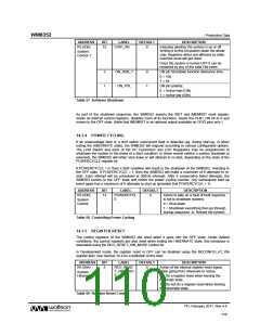
ADDRESS
BIT
LABEL
DEFAULT
DESCRIPTION
R3 (03h)
11:10
RSTB_TO
[1:0]
11
Time that the /RST pin and /MEMRST
output is held low after the chip reaches the
active state.
System
Control 1
00 = 15ms
01 = 30ms
10 = 60ms
11 = 120ms
5
MEM_VALID
0
Indicates that the contents of external
memory are still valid.
This bit is cleared on startup and whenever
/MEMRST is asserted from the main state
machine. The system software should set
this bit once the external memory has been
set up.
Controlled in hibernate mode by
MEMRST_HIB_MODE
0 = External memory is not valid and needs
restoring.
1 = External memory is valid.
/RST pin state in hibernate mode:
0 = Asserted (low)
R5 (05h)
4
2
RST_HIB_M
ODE
0
0
System
Hibernate
1 = Not asserted (high)
MEMRST_H
IB_MODE
/MEMRST (Alternative GPIO function) pin
state in hibernate mode
0 = Asserted (low)
1 = Not asserted (high)
Table 60 Controlling Reset Signals
The WM8352 can be commanded to assert the /RST and /MEMRST signals by writing a logic ‘1’ to
the SYS_RST register bit. In this case, the /RST and /MEMRST outputs are asserted low for the
duration specified by RSTB_TO.
Care must be taken if writing to this bit in 2-wire (I2C) Control Interface mode. The WM8352 will act
upon the register write operation as soon as it has received the address and data fields; this may
PD, February 2011, Rev 4.4
111
w

 WOLFSON [ WOLFSON MICROELECTRONICS PLC ]