Production Data
WM8352
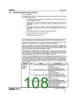
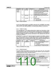
ADDRESS
BIT
LABEL
DESCRIPTION
2
WKUP_GP_PWR_ON_EINT
PWR_ON (Alternate GPIO function) pin
has been pressed for longer than
specified time.
(Rising Edge triggered)
Note: This bit is cleared once read.
1
0
WKUP_ONKEY_EINT
ON key has been pressed for longer than
specified time.
(Rising Edge triggered)
Note: This bit is cleared once read.
WKUP_GP_WAKEUP_EINT
WAKEUP (Alternate GPIO function) pin
has been pressed for longer than
specified time.
(Rising Edge triggered)
Note: This bit is cleared once read.
Interrupt mask.
R39 (27h)
6:0
“IM_” + name of respective
bit in R31
Comparator
Interrupt
Status Mask
0 = Do not mask interrupt.
1 = Mask interrupt.
Each bit in R39 enables or masks the
corresponding bit in R31. The default
value for these bits is 0 (unmasked).
Table 56 Wake-Up Interrupts
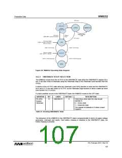
14.3.2 POWER-UP SEQUENCING
The WM8352 power supply blocks can be commanded to start up according to a defined sequence
when the WM8352 is commanded into the ACTIVE state. This sequence comprises fourteen
timeslots, where the enabling of each DC-DC converter, LDO voltage regulator and the current limit
switch is associated with one timeslot. In order to minimise supply in-rush current at power-up time,
the start-up of these power supply blocks should be staggered in time by the use of this feature.
The WM8352 proceeds from one time slot to the next after a delay of approximately 1.28ms,
provided that all power supply blocks started up in the current time slot (if any) have reached 90% of
their programmed output voltage. See Section 14.3.4 for details of the WM8352 behaviour if any
power supply block fails to achieve 90% of its programmed output voltage.
14.3.3 SHUTDOWN
The WM8352 goes from ACTIVE or HIBERNATE to the OFF state when a shutdown event occurs.
Shutdown events include:
.
.
Software shutdown (setting CHIP_ON = 0)
A trigger signal on a GPIO pin configured as PWR_OFF lasting more than 5ms. The active
polarity of this input is set by GPn_CFG for the applicable GPIO pin (see Section 20).
.
A trigger signal on the ON pin lasting more than 10 seconds. The active polarity of this
input is set by the register field ON_POL. If required, the de-bounce time can be set to 5
seconds using the ON_DEB_T register bit.
.
.
.
Watchdog time-out (see Section 23) after 7 previous faults.
Fault conditions programmed to trigger a shutdown (see Section 18).
Thermal shutdown (see Section 25)
As part of the start-up sequence, the CHIP_ON bit is set to 1. The software shutdown is commanded
by writing 0 to the CHIP_ON register field as described in Table 57.
PD, February 2011, Rev 4.4
109
w

 WOLFSON [ WOLFSON MICROELECTRONICS PLC ]