WM8352
Production Data
REGISTER
15
14
13
12
11
10
9
8
7
6
5
4
3
2
1
0
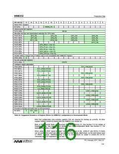
Select /RST duration
R3 (03h)
RSTB_TO
Unlock protected registers
R219 (DBh)
0013h
Alternate function and input/output selection for GPIO pins
R140 (8Ch)
R141 (8Dh)
R142 (8Eh)
R143 (8Fh)
R128 (80h)
R129 (81h)
R130 (82h)
R134 (86h)
R135 (87h)
GP3_FN
GP7_FN
GP11_FN
GP2_FN
GP6_FN
GP10_FN
GP1_FN
GP5_FN
GP9_FN
GP0_FN
GP4_FN
GP8_FN
GP12_FN
GPn_DB (n = 0 to 12)
GPn_PU (n = 0 to 12)
GPn_PD (n = 0 to 12)
GPn_DIR (n = 0 to 12)
GPn_CFG (n = 0 to 12)
Disable battery charger (only if battery type is not compatible with WM8352 charger)
R168 (A8h)
0
Re-lock protected registers
R219 (DBh)
FFFFh
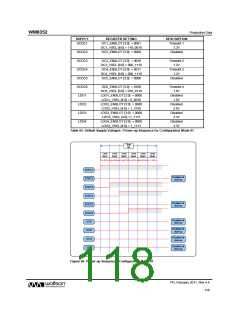
Configure supply generation
R180 (B4h)
DC1_VSEL[6:0]
R181(B5h)
DC1_ENSLOT[3:0]
DC2_ENSLOT[3:0]
R183 (B7h)
R186 (BAh)
DC3_VSEL[6:0]
DC4_VSEL[6:0]
R187 (BBh)
DC3_ENSLOT 3:0]
R189 (BDh)
R190 (BEh)
DC4_ENSLOT[3:0]
DC5_ENSLOT[3:0]
R193 (C1h)
R195 (C3h)
DC6_VSEL[6:0]
R196 (C4h)
DC6_ENSLOT[3:0]
LS_ENSLOT[3:0]
R199 (C7h)
R200 (C8h)
LDO1_VSEL[4:0]
R201 (C9h)
LDO1_ENSLOT[3:0]
LDO2_ENSLOT[3:0]
LDO3_ENSLOT[3:0]
LDO4_ENSLOT[3:0]
R203 (CAh)
LDO2_VSEL[4:0]
LDO3_VSEL[4:0]
LDO4_VSEL[4:0]
R204 (CBh)
R206 (CEh)
R207 (CFh)
R209 (D1h)
R210 (D2h)
Proceed to startup and hand over to host processor
R6 (06h)
0
DEV_ADD
R
1
Table 64 Suggested Sequence of Register Writes for WM8352 Configuration in Development Mode
Note that configuration only includes registers that are required for starting up correctly. All other
register settings should be loaded after the WM8352 has started up.
Most of these control fields are described here within Section 14. See Section 11.6 for details of
Register Locking. See Section 20 for details of the GPIO configuration fields. See Section 17.7 for
details of the Battery Charger configuration.
When using the /RST signal to trigger configuration, writing to the _ENSLOT and RSTB_TO fields
can be omitted (the reset and power-up sequence has already taken place, so the write would have
no effect). However, additional writes to R13 or R176 should be added to enable the DC-DC
converters and LDO regulators one by one.
PD, February 2011, Rev 4.4
116
w

 WOLFSON [ WOLFSON MICROELECTRONICS PLC ]