W9825G6KH
7.5 Burst Read Command
The Burst Read command is initiated by applying logic low level to CS and CAS while holding
RAS and WE high at the rising edge of the clock. The address inputs determine the starting
column address for the burst. The Mode Register sets type of burst (sequential or interleave) and the
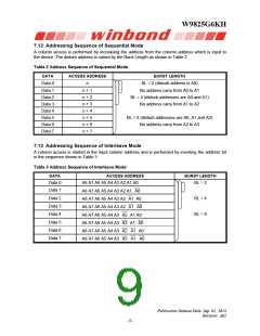
burst length (1, 2, 4, 8 and full page) during the Mode Register Set Up cycle. Table 2 and 3 in the next
page explain the address sequence of interleave mode and sequential mode.
7.6 Burst Write Command
The Burst Write command is initiated by applying logic low level to CS
,
CAS and WE while
holding RAS high at the rising edge of the clock. The address inputs determine the starting column
address. Data for the first burst write cycle must be applied on the DQ pins on the same clock cycle
that the Write Command is issued. The remaining data inputs must be supplied on each subsequent
rising clock edge until the burst length is completed. Data supplied to the DQ pins after burst finishes
will be ignored.
7.7 Read Interrupted by a Read
A Burst Read may be interrupted by another Read Command. When the previous burst is interrupted,
the remaining addresses are overridden by the new read address with the full burst length. The data
from the first Read Command continues to appear on the outputs until the CAS Latency from the
interrupting Read Command the is satisfied.
7.8 Read Interrupted by a Write
To interrupt a burst read with a Write Command, DQM may be needed to place the DQs (output
drivers) in a high impedance state to avoid data contention on the DQ bus. If a Read Command will
issue data on the first and second clocks cycles of the write operation, DQM is needed to insure the
DQs are tri-stated. After that point the Write Command will have control of the DQ bus and DQM
masking is no longer needed.
7.9 Write Interrupted by a Write
A burst write may be interrupted before completion of the burst by another Write Command. When the
previous burst is interrupted, the remaining addresses are overridden by the new address and data
will be written into the device until the programmed burst length is satisfied.
7.10 Write Interrupted by a Read
A Read Command will interrupt a burst write operation on the same clock cycle that the Read
Command is activated. The DQs must be in the high impedance state at least one cycle before the
new read data appears on the outputs to avoid data contention. When the Read Command is
activated, any residual data from the burst write cycle will be ignored.
7.11 Burst Stop Command
A Burst Stop Command may be used to terminate the existing burst operation but leave the bank open
for future Read or Write Commands to the same page of the active bank. The Burst Stop Command is
defined by having RAS and CAS high with CS and WE low at the rising edge of the clock. The
data DQs go to a high impedance state after a delay which is equal to the CAS Latency in a burst read
cycle interrupted by Burst Stop.
Publication Release Date: Sep. 01, 2014
Revision: A02
- 8 -

 WINBOND [ WINBOND ]