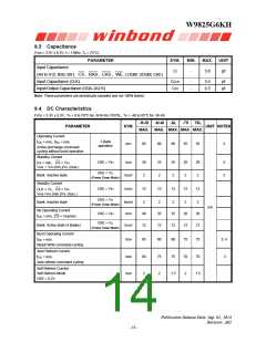
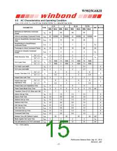
W9825G6KH
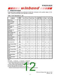
8. OPERATION MODE
Fully synchronous operations are performed to latch the commands at the positive edges of CLK.
Table 1 shows the truth table for the operation commands.
Table 1 Truth Table (Note (1) , (2))
DEICE
STATE
A0A9
COMMAND
Bank Active
CKEn-1 CKEn DQM BS0, 1 A10
CS RAS CAS
WE
A11, A12
Idle
Any
H
H
H
H
x
x
x
x
x
x
x
x
v
v
x
v
v
L
H
L
v
x
x
v
L
L
L
L
L
L
H
H
H
L
H
L
L
L
Bank Precharge
Precharge All
Write
Any
L
Active (3)
H
Write with Auto-
precharge
Active (3)
Active (3)
Active (3)
H
H
H
x
x
x
x
x
x
v
v
v
H
L
v
v
v
L
L
L
H
H
H
L
L
L
L
H
H
Read
Read with Auto-
precharge
H
Mode Register Set
No-operation
Idle
Any
H
H
H
H
H
H
x
x
x
x
x
x
x
x
v
x
x
x
x
x
v
x
x
x
x
x
v
x
x
x
x
x
L
L
L
H
L
L
L
H
H
x
L
H
H
x
L
H
L
Burst Stop
Active (4)
x
Device Deselect
Auto-refresh
Any
x
x
Idle
H
L
L
L
H
H
Self-refresh Entry
Idle
L
L
L
L
H
H
x
x
x
x
x
x
x
x
H
L
x
x
x
x
Idle
(S.R.)
Self-refresh Exit
H
H
Clock Suspend Mode
Entry
Active
H
L
x
x
x
x
x
x
x
x
H
H
L
L
x
x
x
x
x
x
x
x
H
L
x
x
x
x
Power Down Mode
Entry
Idle
Active (5)
H
H
Clock Suspend Mode
Exit
Active
L
H
x
x
x
x
x
x
x
x
L
L
H
H
x
x
x
x
x
x
x
x
H
L
x
x
x
x
Power Down Mode
Exit
Any
(Power Down)
H
H
Data Write/Output
Enable
Active
Active
H
H
x
x
L
x
x
x
x
x
x
x
x
x
x
x
x
x
x
Data Write/Output
Disable
H
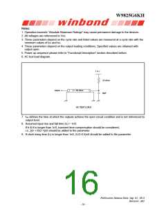
Notes:
(1) v = valid
x = Don't care
L = Low Level H = High Level
(2) CKEn signal is input level when commands are provided.
CKEn-1 signal is the input level one clock cycle before the command is issued.
(3) These are state of bank designated by BS0, BS1 signals.
(4) Device state is full page burst operation.
(5) Power Down Mode can not be entered in the burst cycle.
When this command asserts in the burst cycle, device state is clock suspend mode.
Publication Release Date: Sep. 01, 2014
Revision: A02
- 12 -

 WINBOND [ WINBOND ]