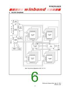
W9825G6KH
7.14 Auto-precharge Command
If A10 is set to high when the Read or Write Command is issued, then the Auto-precharge function is
entered. During Auto-precharge, a Read Command will execute as normal with the exception that the
active bank will begin to precharge automatically before all burst read cycles have been completed.
Regardless of burst length, it will begin a certain number of clocks prior to the end of the scheduled
burst cycle. The number of clocks is determined by CAS Latency.
A Read or Write Command with Auto-precharge can not be interrupted before the entire burst
operation is completed. Therefore, use of a Read, Write, or Precharge Command is prohibited during
a read or write cycle with Auto-precharge. Once the precharge operation has started, the bank cannot
be reactivated until the Precharge time (tRP) has been satisfied. Issue of Auto-pecharge command is
illegal if the burst is set to full page length. If A10 is high when a Write Command is issued, the Write
with Auto-pecharge function is initiated. The SDRAM automatically enters the precharge operation two
clock delay from the last burst write cycle. This delay is referred to as Write tWR. The bank undergoing
Auto-precharge can not be reactivated until tWR and tRP are satisfied. This is referred to as tDAL, Data-in
to Active delay (tDAL = tWR + tRP). When using the Auto-precharge Command, the interval between the
Bank Activate Command and the beginning of the internal precharge operation must satisfy tRAS (min).
7.15 Precharge Command
The Precharge Command is used to precharge or close a bank that has been activated. The
Precharge Command is entered when CS
,
RAS and WE are low and CAS is high at the rising
edge of the clock. The Precharge Command can be used to precharge each bank separately or all
banks simultaneously. Three address bits A10, BS0 and BS1 are used to define which bank(s) is to be
precharged when the command is issued. After the Precharge Command is issued, the precharged
bank must be reactivated before a new read or write access can be executed. The delay between the
Precharge Command and the Activate Command must be greater than or equal to the Precharge time
(tRP).
7.16 Self Refresh Command
The Self Refresh Command is defined by having CS
RAS CAS and CKE held low with WE
, ,
high at the rising edge of the clock. All banks must be idle prior to issuing the Self Refresh Command.
Once the command is registered, CKE must be held low to keep the device in Self Refresh mode.
When the SDRAM has entered Self Refresh mode all of the external control signals, except CKE, are
disabled. The clock is internally disabled during Self Refresh Operation to save power. The device will
exit Self Refresh operation after CKE is returned high. Any subsequent commands can be issued after
tXSR from the end of Self Refresh Command.
If, during normal operation, AUTO REFRESH cycles are issued in bursts (as opposed to being evenly
distributed), a burst of 8,192 AUTO REFRESH cycles should be completed just prior to entering and
just after exiting the self refresh mode.
Publication Release Date: Sep. 01, 2014
Revision: A02
- 10 -

 WINBOND [ WINBOND ]