W9825G6KH
7. FUNCTIONAL DESCRIPTION
7.1 Power Up and Initialization
The default power up state of the mode register is unspecified. The following power up and
initialization sequence need to be followed to guarantee the device being preconditioned to each user
specific needs.
During power up, all VDD and VDDQ pins must be ramp up simultaneously to the specified voltage
when the input signals are held in the “NOP” state. The power up voltage must not exceed VDD + 0.3V
on any of the input pins or VDD supplies. After power up, an initial pause of 200 µS is required followed
by a precharge of all banks using the precharge command. To prevent data contention on the DQ bus
during power up, it is required that the DQM and CKE pins be held high during the initial pause period.
Once all banks have been precharged, the Mode Register Set Command must be issued to initialize
the Mode Register. An additional eight Auto Refresh cycles (CBR) are also required before or after
programming the Mode Register to ensure proper subsequent operation.
7.2 Programming Mode Register
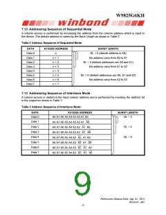
After initial power up, the Mode Register Set Command must be issued for proper device operation.
All banks must be in a precharged state and CKE must be high at least one cycle before the Mode
Register Set Command can be issued. The Mode Register Set Command is activated by the low
signals of RAS
CAS CS and WE at the positive edge of the clock. The address input data
, ,
during this cycle defines the parameters to be set as shown in the Mode Register Operation table. A
new command may be issued following the mode register set command once a delay equal to tRSC
has elapsed. Please refer to the next page for Mode Register Set Cycle and Operation Table.
7.3 Bank Activate Command
The Bank Activate command must be applied before any Read or Write operation can be executed.
The operation is similar to RAS activate in EDO DRAM. The delay from when the Bank Activate
command is applied to when the first read or write operation can begin must not be less than the RAS
to CAS delay time (tRCD). Once a bank has been activated it must be precharged before another Bank
Activate command can be issued to the same bank. The minimum time interval between successive
Bank Activate commands to the same bank is determined by the RAS cycle time of the device (tRC).
The minimum time interval between interleaved Bank Activate commands (Bank A to Bank B and vice
versa) is the Bank to Bank delay time (tRRD). The maximum time that each bank can be held active is
specified as tRAS (max).
7.4 Read and Write Access Modes
After a bank has been activated , a read or write cycle can be followed. This is accomplished by
setting RAS high and CAS low at the clock rising edge after minimum of tRCD delay. WE pin
voltage level defines whether the access cycle is a read operation ( WE high), or a write operation
(
WE low). The address inputs determine the starting column address.
Reading or writing to a different row within an activated bank requires the bank be precharged and a
new Bank Activate command be issued. When more than one bank is activated, interleaved bank
Read or Write operations are possible. By using the programmed burst length and alternating the
access and precharge operations between multiple banks, seamless data access operation among
many different pages can be realized. Read or Write Commands can also be issued to the same bank
or between active banks on every clock cycle.
Publication Release Date: Sep. 01, 2014
Revision: A02
- 7 -

 WINBOND [ WINBOND ]