W9825G6KH
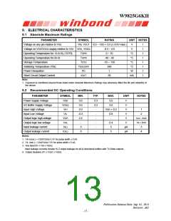
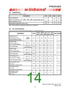
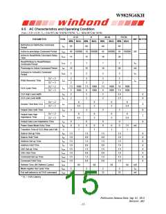
9. ELECTRICAL CHARACTERISTICS
9.1 Absolute Maximum Ratings
PARAMETER
Voltage on any pin relative to VSS
Voltage on VDD/VDDQ supply relative to VSS
Operating Temperature for -5/-6/-6L/-75/75L
Operating Temperature for-5I/-6I
Storage Temperature
SYMBOL
RATING
UNIT NOTES
VIN, VOUT -0.5 ~ VDD + 0.5 (≤ 4.6V max.)
V
V
1
1
1
1
1
1
1
1
-0.5 ~ 4.6
0 ~ 70
-40 ~ 85
-55 ~ 150
260
VDD, VDDQ
TOPR
°C
°C
°C
°C
W
TOPR
TSTG
Soldering Temperature (10s)
Power Dissipation
TSOLDER
PD
1
Short Circuit Output Current
IOUT
50
mA
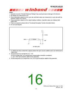
Note:
1. Exposure to conditions beyond those listed under Absolute Maximum Ratings may adversely affect the life and reliability of
the device
9.2 Recommended DC Operating Conditions
PARAMETER
SYMBOL
MIN.
TYP.
MAX.
UNIT
NOTES
Power Supply Voltage
I/O Buffer Supply Voltage
Input High Voltage
VDD
VDDQ
VIH
3.0
3.0
2.0
-0.3
2.4
-
3.3
3.6
V
V
3.3
3.6
-
-
-
-
-
-
VDD + 0.3
V
1
Input Low Voltage
VIL
0.8
-
V
2
IOH= -2mA
Output logic high voltage
Output logic low voltage
Input leakage current
Output leakage current
Notes:
VOH
VOL
II(L)
V
IOL= 2mA
0.4
5
V
-5
µA
µA
3
4
IO(L)
-5
5
1. VIH (max.) = VDD/VDDQ+1.5V for pulse width ≤ 5 nS.
2. VIL (min.) = VSS/VSSQ-1.5V for pulse width ≤ 5 nS.
3. Any input 0V ≤ VIN ≤ VDDQ.
Input leakage currents include Hi-Z output leakage for all bi-directional buffers with Tri-State outputs.
4. Output disabled, 0V ≤ VOUT ≤ VDDQ.
Publication Release Date: Sep. 01, 2014
Revision: A02
- 13 -

 WINBOND [ WINBOND ]