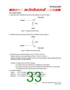
W9412G6JH
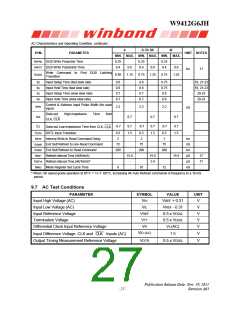
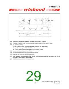
CLK
VX
VX
VICK
VICK
VX
VX
VX
VID(AC)
CLK
VSS
VICK
VICK
VID(AC)
0 V Differential
VISO
VSS
VISO(min)
VISO(max)
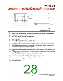
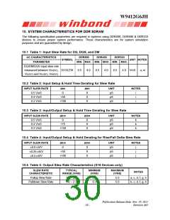
(16) tAC and tDQSCK depend on the clock jitter. These timing are measured at stable clock.
(17) A maximum of eight AUTO REFRESH commands can be posted to any given DDR SDRAM device.
(18) tDAL = (tWR/tCK) + (tRP/tCK)
For each of the terms above, if not already an integer, round to the next highest integer.
Example: For -5 speed grade at CL=2.5 and tCK=6 nS
tDAL = ((15 nS / 6 nS) + (15 nS / 6 nS)) clocks = ((3) + (3)) clocks = 6 clocks
(19) For command/address input slew rate ≥1.0 V/nS.
(20) For command/address input slew rate ≥0.5 V/nS and <1.0 V/nS.
(21) For CLK & CLK slew rate ≥1.0 V/nS (single--ended).
(22) These parameters guarantee device timing, but they are not necessarily tested on each device. They may be
guaranteed by device design or tester correlation.
(23) Slew Rate is measured between VOH(ac) and VOL(ac).
Publication Release Date: Nov. 29, 2011
- 29 -
Revision A03

 WINBOND [ WINBOND ]