W9412G6JH
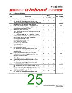
9.5 DC Characteristics
MAX.
SYM.
PARAMETER
UNIT NOTES
-6I
-4
-5/-5I/-5K
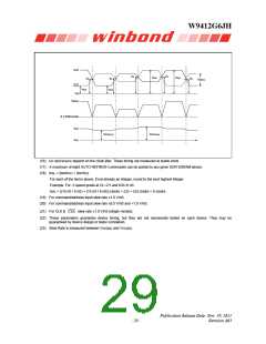
Operating current: One Bank Active-Precharge;
tRC = tRC min; tCK = tCK min;
DQ, DM and DQS inputs changing once per clock cycle;
Address and control inputs changing once every two clock cycles.
IDD0
60
55
50
7
Operating current: One Bank Active-Read-Precharge;
Burst = 4; tRC = tRC min; CL = 3; tCK = tCK min; IOUT = 0 mA;
IDD1
75
5
65
5
55
5
7, 9
Address and control inputs changing once per clock cycle.
Precharge Power Down standby current:
All Banks Idle; Power down mode;
IDD2P
CKE < VIL max; tCK = tCK min; Vin = VREF for DQ, DQS and DM.
Idle standby current:
> VIH min; All Banks Idle; CKE > VIH min; tCK = tCK min;
CS
IDD2N
IDD3P
25
15
20
10
20
10
7
Address and other control inputs changing once per clock cycle;
Vin > VIH min or Vin < VIL max for DQ, DQS and DM.
Active Power Down standby current:
One Bank Active; Power down mode;
CKE < VIL max; tCK = tCK min;
Vin = VREF for DQ, DQS and DM.
Active standby current:
> VIH min; CKE > VIH min; One Bank Active-Precharge;
mA
CS
IDD3N
35
30
30
7
tRC = tRAS max; tCK = tCK min;
DQ, DM and DQS inputs changing twice per clock cycle;
Address and other control inputs changing once per clock cycle.
Operating current:
Burst = 2; Reads; Continuous burst; One Bank Active;
Address and control inputs changing once per clock cycle;
CL=2; tCK = tCK min; IOUT = 0mA.
IDD4R
IDD4W
140
135
120
115
110
100
7, 9
Operating current:
Burst = 2; Write; Continuous burst; One Bank Active;
Address and control inputs changing once per clock cycle;
CL = 2; tCK = tCK min;
7
7
DQ, DM and DQS inputs changing twice per clock cycle.
IDD5
IDD6
Auto Refresh current: tRC = tRFC min.
75
2
70
2
65
2
Self Refresh current: CKE < 0.2V; external clock on; tCK = tCK
min.
Random Read current: 4 Banks Active Read with activate every
20nS, Auto-Precharge Read every 20 nS;
Burst = 4; tRCD = 3; IOUT = 0mA;
IDD7
170
150
130
DQ, DM and DQS inputs changing twice per clock cycle;
Address changing once per clock cycle.
Publication Release Date: Nov. 29, 2011
Revision A03
- 25 -

 WINBOND [ WINBOND ]