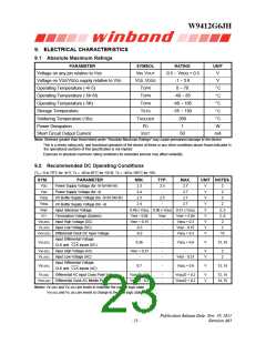
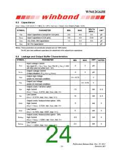
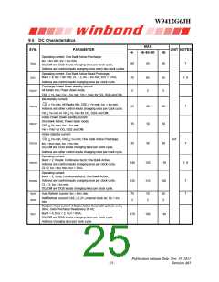
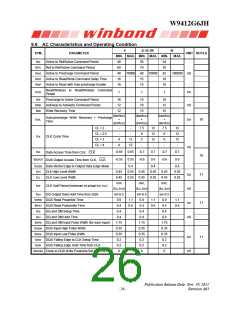
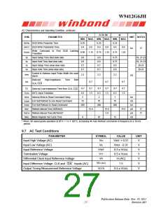
W9412G6JH
AC Characteristics and Operating Condition, continued
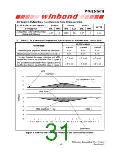
SYM. PARAMETER
-4
-5/-5I/-5K
-6I
UNIT NOTES
MIN. MAX. MIN. MAX. MIN. MAX.
tWPRE DQS Write Preamble Time
tWPST DQS Write Postamble Time
0.25
0.4
0.25
0.4
0.25
0.4
0.6
0.6
0.6
tCK
11
Write Command to First DQS Latching
Transition
tDQSS
0.85
1.15
0.75
1.25
0.75
1.25
tIS
tIH
tIS
tIH
Input Setup Time (fast slew rate)
Input Hold Time (fast slew rate)
Input Setup Time (slow slew rate)
Input Hold Time (slow slew rate)
0.6
0.6
0.7
0.7
0.6
0.6
0.7
0.7
0.75
0.75
0.8
19, 21-23
19, 21-23
20-23
0.8
20-23
Control & Address Input Pulse Width (for each
input)
tIPW
2.2
2.2
2.2
nS
Data-out
High-impedance
Time
from
tHZ
tLZ
0.7
0.7
0.7
CLK, CLK
-0.7
0.7
1.5
-0.7
0.7
1.5
-0.7
0.7
1.5
Data-out Low-impedance Time from CLK, CLK
tT(SS) SSTL Input Transition
0.5
2
0.5
2
0.5
1
tWTR
Internal Write to Read Command Delay
tCK
nS
tCK
µS
µS
nS
tXSNR Exit Self Refresh to non-Read Command
tXSRD Exit Self Refresh to Read Command
72
200
75
200
75
200
tREFi
Refresh Interval Time (4K/64mS)
tREFiA Refresh Interval Time (4K/16mS)*
Mode Register Set Cycle Time
15.6
-
15.6
3.9
15.6
-
17
17
tMRD
8
10
12
* When -5K speed grade operation at 85°C < TA ≤ 105°C, increasing 4K Auto Refresh commands in frequency to a 16 mS
period.
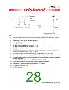
9.7 AC Test Conditions
PARAMETER
Input High Voltage (AC)
SYMBOL
VIH
VALUE
VREF + 0.31
VREF - 0.31
0.5 x VDDQ
0.5 x VDDQ
Vx (AC)
UNIT
V
Input Low Voltage (AC)
VIL
V
Input Reference Voltage
VREF
VTT
V
Termination Voltage
V
Differential Clock Input Reference Voltage
VR
V
VID (AC)
1.5
V
V
Input Difference Voltage. CLK and CLK Inputs (AC)
Output Timing Measurement Reference Voltage
VOTR
0.5 x VDDQ
Publication Release Date: Nov. 29, 2011
Revision A03
- 27 -

 WINBOND [ WINBOND ]