W9412G6JH
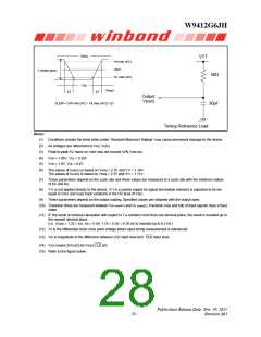
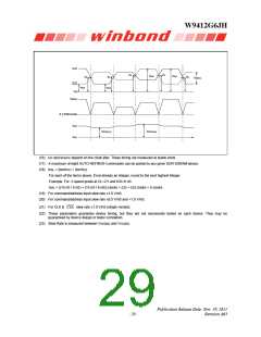
9.6 AC Characteristics and Operating Condition
-4
-5/-5I/-5K
-6I
SYM.
PARAMETER
UNIT NOTES
MAX.
MIN. MAX. MIN. MAX. MIN.
tRC
Active to Ref/Active Command Period
Ref to Ref/Active Command Period
48
60
40
16
16
50
70
40
15
15
54
70
42
18
18
tRFC
tRAS
tRCD
tRAP
Active to Precharge Command Period
Active to Read/Write Command Delay Time
Active to Read with Auto-precharge Enable
70000
70000
100000 nS
Read/Write(a) to Read/Write(b) Command
Period
tCCD
1
1
1
tCK
nS
tRP
tRRD
tWR
Precharge to Active Command Period
Active(a) to Active(b) Command Period
Write Recovery Time
16
12
12
15
10
15
18
12
15
(tWR/tCK)
+
(tRP/tCK)
(tWR/tCK)
+
(tRP/tCK)
(tWR/tCK)
+
(tRP/tCK)
Auto-precharge Write Recovery + Precharge
Time
tDAL
tCK
18
CL = 2
-
-
-
7.5
6
12
12
12
-
7.5
6
12
12
12
-
CL = 2.5
-
tCK
CLK Cycle Time
CL = 3
4
4
12
12
5
6
CL = 4
-
-
nS
tAC
-0.65
-0.55
0.65
0.55
-0.7
-0.6
0.7
0.6
-0.7
-0.6
0.7
0.6
Data Access Time from CLK, CLK
16
11
tDQSCK
DQS Output Access Time from CLK, CLK
tDQSQ Data Strobe Edge to Output Data Edge Skew
0.4
0.4
0.4
tCH
tCL
CLk High Level Width
CLK Low Level Width
0.45
0.45
min
0.55
0.55
0.45
0.45
min,
(tCL,tCH)
tHP-0.5
0.9
0.55
0.55
0.45
0.45
min,
(tCL,tCH)
tHP-0.5
0.9
0.55
0.55
tCK
nS
tCK
nS
tHP
CLK Half Period (minimum of actual tCH, tCL)
(tCL,tCH)
tHP-0.5
0.9
tQH
DQ Output Data Hold Time from DQS
tRPRE DQS Read Preamble Time
tRPST DQS Read Postamble Time
1.1
0.6
1.1
0.6
1.1
0.6
11
0.4
0.4
0.4
tDS
tDH
DQ and DM Setup Time
DQ and DM Hold Time
0.4
0.4
0.4
0.4
0.4
0.4
tDIPW DQ and DM Input Pulse Width (for each input)
tDQSH DQS Input High Pulse Width
1.75
0.35
0.35
0.2
1.75
0.35
0.35
0.2
1.75
0.35
0.35
0.2
tDQSL DQS Input Low Pulse Width
tCK
nS
11
tDSS
tDSH
DQS Falling Edge to CLK Setup Time
DQS Falling Edge Hold Time from CLK
0.2
0.2
0.2
tWPRES Clock to DQS Write Preamble Set-up Time
0
0
0
Publication Release Date: Nov. 29, 2011
Revision A03
- 26 -

 WINBOND [ WINBOND ]