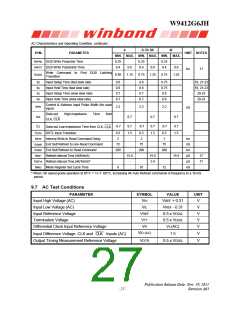
W9412G6JH
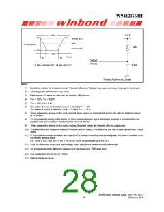
VDDQ
VTT
VIH min (AC)
VREF
V SWING (MAX)
50Ω
VIL max (AC)
VSS
Output
ΔT
ΔT
Output
V(out)
SLEW = (VIH min (AC) - VILmax (AC)) / ΔT
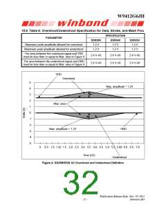
30pF
Timing Reference Load
Notes:
(1) Conditions outside the limits listed under “Absolute Maximum Ratings” may cause permanent damage to the device.
(2)
(3)
(4)
(5)
(6)
All voltages are referenced to VDD, VDDQ.
Peak to peak AC noise on VREF may not exceed 2% VREF(DC).
VOH = 1.95V, VOL = 0.35V
VOH = 1.9V, VOL = 0.4V
The values of IOH(DC) is based on VDDQ = 2.3V and VTT = 1.19V.
The values of IOL(DC) is based on VDDQ = 2.3V and VTT = 1.11V.
(7) These parameters depend on the cycle rate and these values are measured at a cycle rate with the minimum values
of tCK and tRC.
(8) VTT is not applied directly to the device. VTT is a system supply for signal termination resistors is expected to be set
equal to VREF and must track variations in the DC level of VREF.
(9) These parameters depend on the output loading. Specified values are obtained with the output open.
(10) Transition times are measured between VIH min(AC) and VIL max(AC).Transition (rise and fall) of input signals have a fixed
slope.
(11) IF the result of nominal calculation with regard to Tck contains more than one decimal place, the result is rounded up to
the nearest decimal place.
(i.e., tDQSS = 1.25 tCK, tCK = 5 nS, 1.25 5 nS = 6.25 nS is rounded up to 6.2 nS.)
(12) VX is the differential clock cross point voltage where input timing measurement is referenced.
(13) VID is magnitude of the difference between CLK input level and CLK input level.
(14) VISO means {VICK(CLK)+VICK( CLK )}/2.
(15) Refer to the figure below.
Publication Release Date: Nov. 29, 2011
- 28 -
Revision A03

 WINBOND [ WINBOND ]