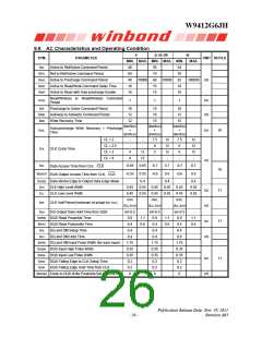
W9412G6JH
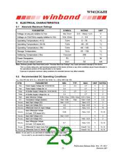
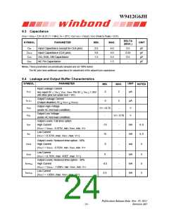
9.3 Capacitance
(VDD = VDDQ = 2.5V 0.2V, f = 1 MHz, TA = 25°C, VOUT (DC) = VDDQ/2, VOUT (Peak to Peak) = 0.2V)
DELTA
UNIT
SYMBOL
PARAMETER
MIN.
MAX.
(MAX.)
CIN
CCLK
CI/O
CNC
Input Capacitance (except for CLK pins)
Input Capacitance (CLK pins)
DQ, DQS, DM Capacitance
NC Pin Capacitance
2.0
3.0
1.5
-
4.0
5.0
5.5
1.5
0.5
0.25
0.5
-
pF
pF
pF
pF
Notes: These parameters are periodically sampled and not 100% tested.
The NC pins have additional capacitance for adjustment of the adjacent pin capacitance.
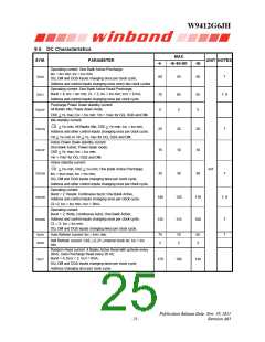
9.4 Leakage and Output Buffer Characteristics
SYMBOL
PARAMETER
UNIT
MIN.
MAX.
NOTES
Input Leakage Current
II (L)
-2
2
µA
Any input 0V < VIN < VDD, VREF Pin 0V < VIN < 1.35V
(All other pins not under test = 0V)
Output Leakage Current
IO (L)
VOH
VOL
-5
5
µA
V
(Output disabled, 0V < VOUT < VDDQ)
Output High Voltage
VTT +0.76
-
-
(under AC test load condition)
Output Low Voltage
VTT -0.76
V
(under AC test load condition)
Output Levels: Full drive option
High Current
IOH
IOL
-15
15
-
-
mA
mA
4, 6
4, 6
(VOUT = VDDQ - 0.373V, min. VREF, min. VTT
Low Current
(VOUT = 0.373V, max. VREF, max. VTT)
Output Levels: Reduced drive option - 60%
High Current
IOHR
-9
-
mA
5
(VOUT = VDDQ - 0.763V, min. VREF, min. VTT
Low Current
IOLR
9
-
-
-
mA
mA
mA
5
5
5
(VOUT = 0.763V, max. VREF, max. VTT)
Output Levels: Reduced drive option - 30%
High Current
IOHR(30)
IOLR(30)
-4.5
4.5
(VOUT = VDDQ – 1.056V, min. VREF, min. VTT
Low Current
(VOUT = 1.056V, max. VREF, max. VTT)
Publication Release Date: Nov. 29, 2011
Revision A03
- 24 -

 WINBOND [ WINBOND ]