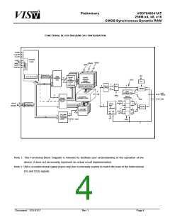
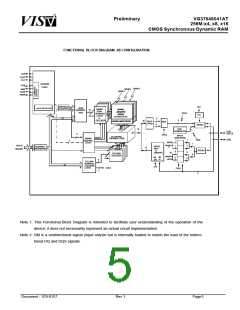
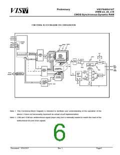
Preliminary
VG37648041AT
256M:x4, x8, x16
VIS
CMOS Synchronous Dynamic RAM
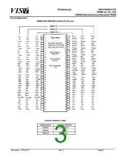
PIN DESCRIPTIONS
Symbol
Type Description
CLIK,CLK#
Input Clock: CLK and CLK# are differential clock inputs. All address and control input signals
are sampled on the positive edge of CLK/negative edge of CLK#. Ouptut(read) data is
referenced to both edges of CLK. Internal clock signals are dervied from CLK/CLK#.
CKE
Input Clock Enable: CKE HIGH activates, and CKE LOW deactivates internal clock signals,
and device input buffers and output drivers. Deactivating the clock provides PRE-
CHARGE POWER-DOWN and SELF REFRESH operation (all banks idle), or ACTIVE
POWER-DOWN (row ACTIVE in any bank). CKE is synchronous for all functions
except for disabling outputs, which is achieved asynchronously. Input buffers, excluding
CLK, CLK# and CKE are disabled during power-down and self refresh modes, provid-
ing low standby power. CKE will recognize an LVCMOS LOW level prior to VREF being
stable on power-up.
CS#
Input Chip Select: CS# enables (registered LOW) and disables (registered HIGH) the com-
mand decoder. All commands are masked when CS# is registered HIGH. CS# provides
for external bank selection on systems with multiple banks. CS# is considered part of
the command code.
RAS#,CAS#,
WE#
Input Command Inputs: RAS#, CAS# and WE# (along with CS#) define the command being
entered.
DM
Input Input Data Mask: DM is an input mask signal for write data. Input data is masked when
DM is sampled HIGH along with that input data during a WRITE access. DM is sampled
on both edges of DQS. DM pins include dummy loading internally, to match the DQ and
DQS loading. For the x16, LDM corresponds to the data on DQ0-DQ7; UDM corre-
sponds to the data on DQ8-DQ15.
BA0,BA1
A0-A12
Input Bank Address Inputs: BA0 and BA1 define to which bank an ACTIVE, READ, WRITE or
PRECHARGE command is being applied.
Input Address Inputs: Provide the row address for ACTIVE commands, and the column
address and AUTO PRECHARGE bit for READ/WRITE commands, to select one loca-
tion out of the memory array in the respective bank. A10 is sampled during a PRE-
CHARGE command to determine whether the PRECHARGE applies to one bank (A10
LOW) or all banks (A10 HIGH). If only one bank is to be precharged, the bank is
selected by BA0,BA1. The address inputs also provide the op-code durinbg a LOAD
MODE REGISTER command.
DQ
I/O
I/O
Data Input/Output: Data bus
DQS
Data Strobe: Output with read data, input with write data. Edge-aligned with read data,
centered in write data. Used to capture write data. For the x16, LDQS corresponds to
the data on DQ0-DQ7; UDQS corresponds to the data on DQ8-DQ15.
NC
-
No Connect: these pins should be left unconnected.
VDDQ
VSSQ
VDD
Supply
DQ Power Supply:+2.5V ±0.2V .
Supply DQ Ground.
Supply
Power Supply: +3.3V ±0.3V .
VSS
Supply Ground.
VREF
Input SSTL_2 reference voltage.
Document : 1G5-0157
Rev.1
Page7

 VML [ VANGUARD INTERNATIONAL SEMICONDUCTOR ]