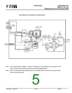
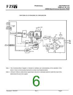
Preliminary
VG37648041AT
256M:x4, x8, x16
VIS
CMOS Synchronous Dynamic RAM
Once in the idle state, two AUTO REFRESH cycles must be performed. Additionally, a LOAD
MODE REGISTER command for the base Mode Register, with the reset DLL bit deactivated (i.e.
to program operating parameters without resetting the DLL) must be performed. Following these
cycles, the DDR SDRAM is ready for normal operation.
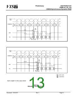
Register Definition
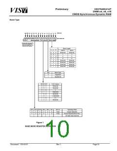
Base Mode Register
The base mode register is used to define the specific mode of operation of the DDR SDRAM.
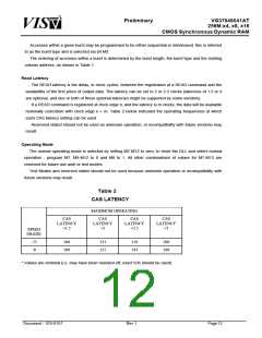
This definition includes the selection of a burst length, a burst type, a CAS latency, and an operat-
ing mode, as shown in Figure 1. The base mode register is programmed via the LOAD MODE
REGISTER command (with BA0=0 and BA1=0) and will retain the stored information unitil it is
programmed again or the device loses power.
Base mode register bits M0-M2 specify the burst length, M3 specifies the type of burst
(sequential or interleaved), M4-M6 specify the CAS latency, and M7-M11 specify the operating
mode.
The base mode register must be loaded when all banks are idle, and the controller must wait
the specified time before initiating the subsequent operation. Violating either of these require-
ments will result in unspecified operation.
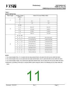
Burst Length
Read and write accesses to the DDR SDRAM are burst oriented, with the burst length being
programmable, as shown in Figure 1. the burst length determines the maximum number of col-
umn locations that can be accessed for a given READ or WRITE command. Burst lengths of 2, 4,
or 8 locations are available for both the sequential and the interleaved burst types.
Reserved states should not be used, as unknown operation or incompatibility with future
versions may result.
When a READ or WRITE command is issued, a block of columns equal to the burst length is
effectively selected. All accesses for that burst take place within this block, meaning that the burst
will wrap within the block if a boundary is reached. The block is uniquely selected by A1-Ai when
the burst length is set to two, by A2-Ai when the burst length is set to four and by A3-Ai when the
burst length is set to eight (where Ai is the most significant column address bit for a given configu-
ration). The remaining (least significant) address bit(s) is (are) used to select the starting location
within the block. The programmed burst length applies to both READ and WRITE bursts.
Document : 1G5-0157
Rev.1
Page9

 VML [ VANGUARD INTERNATIONAL SEMICONDUCTOR ]