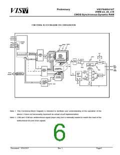
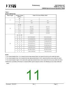
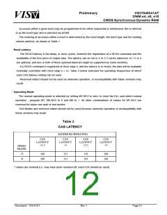
Preliminary
VG37648041AT
256M:x4, x8, x16
VIS
CMOS Synchronous Dynamic RAM
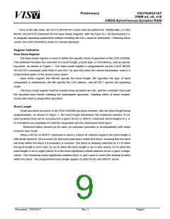
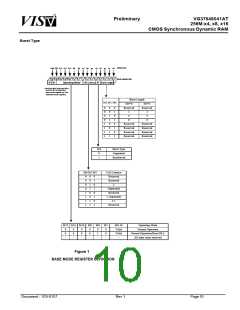
Burst Type
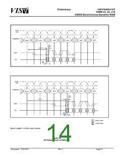
Address Bus
BA0
BA0
A12 A11 A10 A9 A8 A7 A6
A3
A0
A4
A1
A5
A2
0
1
6
4
5
3
2
14
9
8
7
12 11
Mode Register (Mx)
13
10
0* 0*
Operating Mode
CAS Latency BT Burst Length
* M13 and M14 (BA0 and BA1)
must be 0,0 to select the
base mode register (vs. the
extended mode register).
Burst Length
M2 M1 M0
M3=0
Reserved
2
M3=1
0
0
0
0
1
1
1
1
0
0
1
1
0
0
1
1
0
1
0
1
0
1
0
1
Reserved
2
4
4
8
8
Reserved
Reserved
Reserved
Reserved
Reserved
Reserved
Reserved
Reserved
M3
0
Burst Type
Sequential
Interleaved
1
M6 M5 M4
CAS Latency
Reserved
Reserved
2
0
0
0
0
1
1
1
1
0
0
1
1
0
0
1
1
0
1
0
1
0
1
0
1
3(optional)
Reserved
1.5(optional)
2.5
Reserved
M12 M11 M10 M9 M8 M7
M6-10
Valid
Valid
-
Operating Mode
Normal Operation
0
0
-
0
0
-
0
0
-
0
0
-
0
1
-
0
0
-
Normal Operation/Reset DLL
All other states reserved
Figure 1
BASE MODE REGISTER DEFINITION
Document : 1G5-0157
Rev.1
Page10

 VML [ VANGUARD INTERNATIONAL SEMICONDUCTOR ]