VSC8601 Datasheet
Configuration
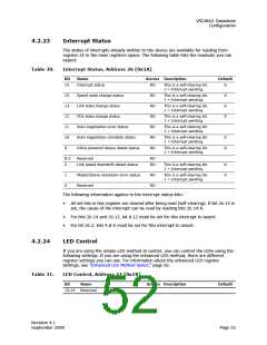
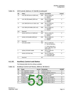
Table 31.
LED Control, Address 27 (0x1B) (continued)
Bit
Name
Access Description
Default
13
Link 100 LED force on (LED2 pin)
R/W
R/W
R/W
R/W
This is a sticky bit.
1 = Forced on.
0 = Default.
0
12
11
10
Link 100 LED disable (LED2 pin)
Link 1000 LED force on (LED1 pin)
Link 1000 LED disable (LED1 pin)
This is a sticky bit.
1 = Disabled.
0 = Default.
0
0
0
This is a sticky bit.
1 = Forced on.
0 = Default.
This is a sticky bit.
1 = Disabled.
0 = Default.
9:8
7
Reserved
RO
Activity LED force on (LED0 pin)
R/W
This is a sticky bit.
1 = Forced on.
0 = Default.
0
0
6
Activity LED disable (LED0 pin)
R/W
This is a sticky bit.
1 = Disabled.
0 = Default.
5:4
3
Reserved
RO
LED pulse enable
RW
This is a sticky bit.
0
0 = Normal operation.
1 = LEDs pulse with a
5 KHz, 20% duty cycle
when active.
2
1
Activity LED blink enable
Activity LED blink rate
RW
RW
This is a sticky bit.
1 = Enable.
0
0
This is a sticky bit.
1 = 10 Hz blink rate.
0 = 5 Hz blink rate.
0
Reserved
RO
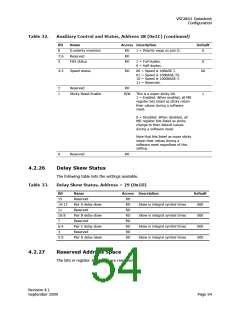
4.2.25
Auxiliary Control and Status
The following table lists the settings available.
Auxiliary Control and Status, Address 28 (0x1C)
Table 32.
Bit
15
14
13
Name
Access Description
Default
Auto-negotiation complete
Auto-negotiation disabled
RO
RO
RO
Duplicate of bit 1.5.
0
0
0
Inverted duplicate of bit 0.12.
MDI/MDI-X crossover
indication
1 = MDI/MDI-X crossover
performed internally.
12
11
10
9
CD pair swap
RO
RO
RO
RO
1 = CD pairs are swapped.
1 = Polarity swap on pair A.
1 = Polarity swap on pair B.
1 = Polarity swap on pair C.
0
0
0
0
A polarity inversion
B polarity inversion
C polarity inversion
Revision 4.1
September 2009
Page 53

 VITESSE [ VITESSE SEMICONDUCTOR CORPORATION ]