New Product
SiS438DN
Vishay Siliconix
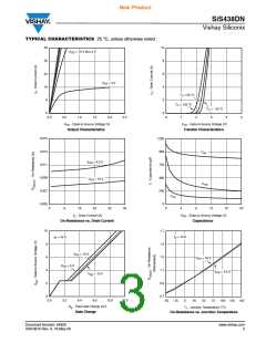
SPECIFICATIONS T = 25 °C, unless otherwise noted
J
Parameter
Symbol
Test Conditions
Min.
Typ.
Max.
Unit
Static
VDS
ΔVDS/TJ
ΔVGS(th)/TJ
VGS(th)
VGS = 0 V, ID = 250 µA
ID = 250 µA
Drain-Source Breakdown Voltage
20
V
V
DS Temperature Coefficient
22
mV/°C
VGS(th) Temperature Coefficient
- 5.0
VDS = VGS , ID = 250 µA
Gate-Source Threshold Voltage
Gate-Source Leakage
1.0
20
2.3
100
1
V
IGSS
VDS = 0 V, VGS
=
20 V
nA
VDS = 20 V, VGS = 0 V
DS = 20 V, VGS = 0 V, TJ = 55 °C
VDS ≥ 5 V, VGS = 10 V
VGS = 10 V, ID = 10 A
IDSS
ID(on)
RDS(on)
gfs
Zero Gate Voltage Drain Current
On-State Drain Currenta
µA
A
V
5
0.0079
0.0102
26
0.0095
0.0125
Drain-Source On-State Resistancea
Ω
S
VGS = 4.5 V, ID = 7 A
Forward Transconductancea
VDS = 10 V, ID = 10 A
Dynamicb
Ciss
Coss
Crss
Input Capacitance
Output Capacitance
Reverse Transfer Capacitance
880
310
125
15
7.3
2.2
2.1
0.9
15
11
16
8
V
DS = 10 V, VGS = 0 V, f = 1 MHz
pF
V
DS = 10 V, VGS = 10 V, ID = 10 A
23
11
Qg
Total Gate Charge
nC
Qgs
Qgd
Rg
Gate-Source Charge
VDS = 15 V, VGS = 4.5 V, ID = 10 A
Gate-Drain Charge
Gate Resistance
f = 1 MHz
0.2
1.8
30
22
30
16
20
16
30
14
Ω
td(on)
tr
td(off)
tf
td(on)
tr
td(off)
tf
Turn-On Delay Time
Rise Time
V
DD = 10 V, RL = 2 Ω
ID ≅ 5 A, VGEN = 4.5 V, Rg = 1 Ω
Turn-Off Delay Time
Fall Time
ns
Turn-On Delay Time
10
8
Rise Time
V
DD = 10 V, RL = 2 Ω
ID ≅ 5 A, VGEN = 10 V, Rg = 1 Ω
Turn-Off Delay Time
16
7
Fall Time
Drain-Source Body Diode Characteristics
Continuous Source-Drain Diode Current
Pulse Diode Forward Current
Body Diode Voltage
IS
ISM
VSD
trr
TC = 25 °C
16
32
1.2
28
9
A
IS = 3 A, VGS = 0 V
0.77
14
V
Body Diode Reverse Recovery Time
Body Diode Reverse Recovery Charge
Reverse Recovery Fall Time
Reverse Recovery Rise Time
ns
nC
Qrr
ta
4.5
5.5
8.5
IF = 10 A, dI/dt = 100 A/µs, TJ = 25 °C
ns
tb
Notes:
a. Pulse test; pulse width ≤ 300 µs, duty cycle ≤ 2 %.
b. Guaranteed by design, not subject to production testing.
Stresses beyond those listed under “Absolute Maximum Ratings” may cause permanent damage to the device. These are stress ratings only, and functional operation
of the device at these or any other conditions beyond those indicated in the operational sections of the specifications is not implied. Exposure to absolute maximum
rating conditions for extended periods may affect device reliability.
www.vishay.com
2
Document Number: 64826
S09-0876-Rev. A, 18-May-09

 VISHAY [ VISHAY ]