AN822
Vishay Siliconix
®
PowerPAK 1212 Mounting and Thermal Considerations
Johnson Zhao
MOSFETs for switching applications are now available
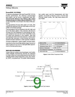
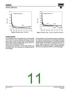
The PowerPAK 1212-8 has a footprint area compara-
ble to TSOP-6. It is over 40 % smaller than standard
TSSOP-8. Its die capacity is more than twice the size
of the standard TSOP-6’s. It has thermal performance
an order of magnitude better than the SO-8, and 20
times better than TSSOP-8. Its thermal performance is
better than all current SMT packages in the market. It
will take the advantage of any PC board heat sink
capability. Bringing the junction temperature down also
increases the die efficiency by around 20 % compared
with TSSOP-8. For applications where bigger pack-
ages are typically required solely for thermal consider-
ation, the PowerPAK 1212-8 is a good option.
with die on resistances around 1 mΩ and with the
capability to handle 85 A. While these die capabilities
represent a major advance over what was available
just a few years ago, it is important for power MOSFET
packaging technology to keep pace. It should be obvi-
ous that degradation of a high performance die by the
package is undesirable. PowerPAK is a new package
technology that addresses these issues. The PowerPAK
1212-8 provides ultra-low thermal impedance in a
small package that is ideal for space-constrained
applications. In this application note, the PowerPAK
1212-8’s construction is described. Following this,
mounting information is presented. Finally, thermal
and electrical performance is discussed.
Both the single and dual PowerPAK 1212-8 utilize the
same pin-outs as the single and dual PowerPAK SO-8.
The low 1.05 mm PowerPAK height profile makes both
versions an excellent choice for applications with
space constraints.
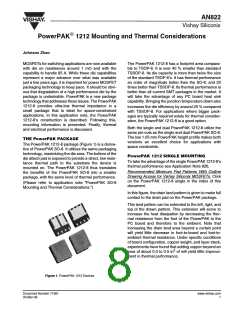
THE PowerPAK PACKAGE
The PowerPAK 1212-8 package (Figure 1) is a deriva-
tive of PowerPAK SO-8. It utilizes the same packaging
technology, maximizing the die area. The bottom of the
die attach pad is exposed to provide a direct, low resis-
tance thermal path to the substrate the device is
mounted on. The PowerPAK 1212-8 thus translates
the benefits of the PowerPAK SO-8 into a smaller
package, with the same level of thermal performance.
PowerPAK 1212 SINGLE MOUNTING
To take the advantage of the single PowerPAK 1212-8’s
thermal performance see Application Note 826,
Recommended Minimum Pad Patterns With Outline
Drawing Access for Vishay Siliconix MOSFETs. Click
on the PowerPAK 1212-8 single in the index of this
document.
(Please refer to application note “PowerPAK SO-8
Mounting and Thermal Considerations.”)
In this figure, the drain land pattern is given to make full
contact to the drain pad on the PowerPAK package.
This land pattern can be extended to the left, right, and
top of the drawn pattern. This extension will serve to
increase the heat dissipation by decreasing the ther-
mal resistance from the foot of the PowerPAK to the
PC board and therefore to the ambient. Note that
increasing the drain land area beyond a certain point
will yield little decrease in foot-to-board and foot-to-
ambient thermal resistance. Under specific conditions
of board configuration, copper weight, and layer stack,
experiments have found that adding copper beyond an
2
area of about 0.3 to 0.5 in of will yield little improve-
ment in thermal performance.
Figure 1. PowerPAK 1212 Devices
Document Number 71681
03-Mar-06
www.vishay.com
1

 VISHAY [ VISHAY ]