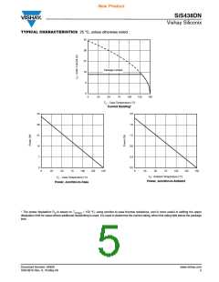
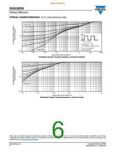
AN822
Vishay Siliconix
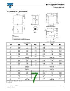
PowerPAK 1212 DUAL
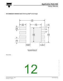
To take the advantage of the dual PowerPAK 1212-8’s
thermal performance, the minimum recommended
land pattern can be found in Application Note 826,
Recommended Minimum Pad Patterns With Outline
Drawing Access for Vishay Siliconix MOSFETs. Click
on the PowerPAK 1212-8 dual in the index of this doc-
ument.
ture profile used, and the temperatures and time
duration, are shown in Figures 2 and 3. For the lead
(Pb)-free solder profile, see http://www.vishay.com/
doc?73257.
The gap between the two drain pads is 10 mils. This
matches the spacing of the two drain pads on the Pow-
erPAK 1212-8 dual package.
This land pattern can be extended to the left, right, and
top of the drawn pattern. This extension will serve to
increase the heat dissipation by decreasing the ther-
mal resistance from the foot of the PowerPAK to the
PC board and therefore to the ambient. Note that
increasing the drain land area beyond a certain point
will yield little decrease in foot-to-board and foot-to-
ambient thermal resistance. Under specific conditions
of board configuration, copper weight, and layer stack,
experiments have found that adding copper beyond an
area of about 0.3 to 0.5 in of will yield little improve-
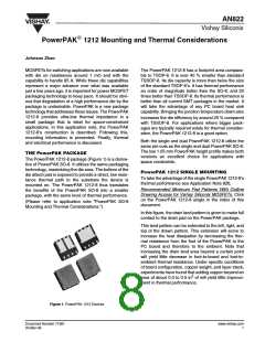
Ramp-Up Rate
+ 6 °C /Second Maximum
2
Temperature at 155 15 °C
Temperature Above 180 °C
Maximum Temperature
Time at Maximum Temperature
Ramp-Down Rate
120 Seconds Maximum
ment in thermal performance.
70 - 180 Seconds
240 + 5/- 0 °C
20 - 40 Seconds
REFLOW SOLDERING
+ 6 °C/Second Maximum
Vishay Siliconix surface-mount packages meet solder
reflow reliability requirements. Devices are subjected
to solder reflow as a preconditioning test and are then
reliability-tested using temperature cycle, bias humid-
ity, HAST, or pressure pot. The solder reflow tempera-
Figure 2. Solder Reflow Temperature Profile
10 s (max)
210 - 220 °C
3 °C/s (max)
4 °C/s (max)
183 °C
140 - 170 °C
50 s (max)
3° C/s (max)
60 s (min)
Reflow Zone
Pre-Heating Zone
Maximum peak temperature at 240 °C is allowed.
Figure 3. Solder Reflow Temperatures and Time Durations
www.vishay.com
2
Document Number 71681
03-Mar-06

 VISHAY [ VISHAY ]