ꢀꢁꢁ ꢂ ꢃꢄ ꢅ ꢆ ꢀꢁꢁ ꢂ ꢃꢄ ꢇ ꢆ ꢀ ꢁꢁ ꢂꢃ ꢄꢄ
ꢀꢁꢁ ꢈ ꢃꢄ ꢅ ꢆ ꢀꢁꢁ ꢈ ꢃꢄ ꢇ ꢆ ꢀ ꢁꢁ ꢈꢃ ꢄꢄ
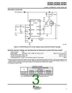
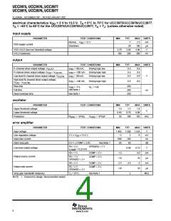
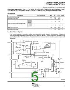
SLUS499A – NOVEMBER 2001 – REVISED JANUARY 2002
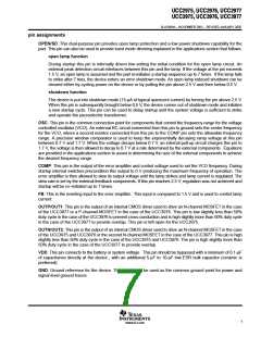
pin assignments
OPEN/SD: This dual-purpose pin provides open lamp protection and a low power shutdown capability for the
part. This pin can also be used to provide burst mode dimming explained in the applications section that follows.
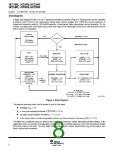
open lamp function
During startup this pin is internally driven low setting the initial condition for the open lamp circuit. An
external peak detection circuit interfaces between this pin and the lamp. If the voltage at the pin exceeds
1.5 V, an open lamp is assumed and the part re-initiates a startup sequence up to 7 times. If the lamp fails
to strike after 7 tries, the device enters an error shutdown mode. An open lamp induced shutdown can be
cleared either by cycling power on the device or by pulling the pin above 2.5 V and then below 0.5 V.
shutdown function
The device is put into shutdown mode (15-µA of typical quiescent current) by forcing the pin above 2.5 V.
When this pin is subsequently brought below 0.5 V, the device comes out of shutdown mode and initiates
a new startup cycle. This pin can be used to delay startup until the system voltage is sufficient to strike
and operate the piezoelectric transformer.
OSC: This pin is the common connection point for components that control the frequency range for the voltage
controlled oscillator (VCO). An external RC circuit connected from this pin to ground sets the center frequency
for the VCO, where a second resistor connected from this pin to the COMP pin sets the allowable frequency
range. A precision window comparator is used to keep the exponentially decaying ramp voltage at this pin
between 0.7 V and 1.7 V. When the voltage decays below 0.7 V, an internal pull-up circuit charges this pin to
1.7 V, the voltage is then allowed to decay to 0.7 V at a rate determined by the external components. Equations
are provided in the applications section to assist in determining the size of the external components to achieve
the desired frequency range.
COMP: This pin is the output of the error amplifier and control voltage used to set the VCO frequency. During
startup internal switches precondition this output to 0 V producing the maximum frequency of operation. The
error amplifier is then allowed to slew its output voltage until the lamp strikes and lamp current is regulated. The
slew rate is set by the external feedback components. If this pin reaches 2.5 V, regulation was not achieved and
startup will be re–initiated up to 7 times.
FB: This is the inverting input to the error amplifier. This input is compared to 1.5 V and is used to control lamp
current.
OUTP/OUT1: This pin is the output of an internal CMOS driver used to drive an N-channel MOSFET in the case
of the UCC3977 or a P-channel MOSFET in the case of the UCC3976. This pin is low slightly less than 50%
duty cycle in the case of the UCC3976 to prevent cross-conduction and is high slightly more than 50% duty cycle
in the case of the UCC3977 to provide overlap. This pin is left open for the UCC3975.
OUTN/OUT2: This pin is the output of an internal CMOS driver used to drive an N-channel MOSFET in the case
of the UCC3975 and UCC3976 or the second N-channel MOSFET in the case of the UCC3977. This pin is high
slightly less than 50% duty cycle in the case of the UCC3975 and UCC3976. The pin is high slightly more than
50% duty cycle in the case of the UCC3977 to provide overlap.
VDD: This pin connects to the battery or system voltage. This pin should be bypassed with a minimum of 0.1-µF
of capacitance directly at the device , with an additional 5-µF to 10-µF low ESR bulk capacitor (ceramic is
preferred).
GND: Ground reference for the device. This pin should be used as the common ground point for power and
signal level ground traces.
7
www.ti.com

 TI [ TEXAS INSTRUMENTS ]