ꢀ ꢁꢁꢂ ꢃ ꢄ ꢅ ꢆ ꢀ ꢁ ꢁꢂ ꢃ ꢄ ꢇ ꢆ ꢀꢁ ꢁꢂ ꢃ ꢄ ꢄ
ꢀ ꢁꢁꢈ ꢃ ꢄ ꢅ ꢆ ꢀ ꢁ ꢁꢈ ꢃ ꢄ ꢇ ꢆ ꢀꢁ ꢁꢈ ꢃ ꢄ ꢄ
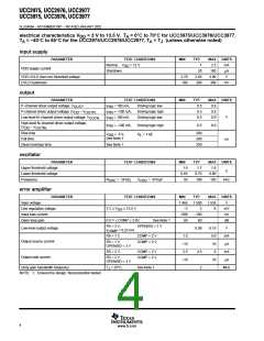
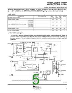
SLUS499A – NOVEMBER 2001 – REVISED JANUARY 2002
electrical characteristics V
A
= 3 V to 13.5 V, T = 0°C to 70°C for UCC3975/UCC3976/UCC3977,
A
DD
T = –40°C to 85°C for the UCC2975/UCC2976/UCC2977, T = T (unless otherwise noted)
A
J
input supply
PARAMETER
TEST CONDITIONS
MIN
TYP
MAX
2.5
UNITS
mA
µA
Normal,
V
= 12 V
1
DD
VDD supply current
Shutdown
20
2.85
200
100
3.00
300
VDD UVLO (turn-on) threshold voltage
UVLO hysteresis
2.70
100
V
mV
output
PARAMETER
TEST CONDITIONS
MIN
TYP
MAX
0.9
UNITS
P–channel driver output voltage, V
I
I
I
= 100 mA,
= –100 mA,
= 100 mA,
Driving logic low
0.5
0.5
0.5
OUTP
– V
PIN
PIN
PIN
P-channel driver output voltage, (V
Driving logic high
Driving logic low
0.9
DD
OUTP)
V
Low-level N–channel driver output voltage, V
0.9
OUTN
High-level N–channel driver output voltage,
I
= –100 mA,
Driving logic high
0.5
0.9
PIN
(V
DD
– V
OUTN)
Rise time
Fall time
200
200
250
V
= 5 V,
C = 1 nF,
L
DD
See Note 1
ns
Dead (overlap) time
See Note 1
oscillator
PARAMETER
TEST CONDITIONS
MIN
1.6
TYP
MAX
1.8
UNITS
Upper threshold voltage
Lower threshold voltage
Frequency
1.7
0.70
100
V
0.65
95
0.80
105
R
= 24 kΩ,
C
= 470 pF
OSC
kHz
OSC
error amplifier
PARAMETER
TEST CONDITIONS
MIN
TYP
MAX
1.535
6
UNITS
V
Input voltage
1.465
–2
1.500
2
Line regulation voltage
Input bias current
Open loop gain
3 V ≤ V
DD
≤ 13.5 V
mV
nA
–500
60
–100
80
0.5 V ≤ COMP ≤ 3.0V,
FB = 2 V, OPEN/SD = 1 V
= 0.23 mA
See Note 1
dB
Low-level output voltage
0.08
0.15
5.0
10
6
V
mA
µA
I
COMP
FB = 1 V,
COMP = 2 V
1.5
–10
2.5
Output source current
FB = 1 V,
COMP = 2 V,
OPEN/SD = 3 V
FB = 2 V,
COMP = 2 V
COMP = 2 V,
4.5
2
mA
µA
Output sink current
FB = 2 V,
–10
10
OPEN/SD = 3 V
Unity gain bandwidth frequency
T
J
= 25°C,
See Note 1
MHz
NOTE: 1. Ensured by design. Not production tested.
4
www.ti.com

 TI [ TEXAS INSTRUMENTS ]