ꢀ ꢁꢁꢂ ꢃ ꢄ ꢅ ꢆ ꢀ ꢁ ꢁꢂ ꢃ ꢄ ꢇ ꢆ ꢀꢁ ꢁꢂ ꢃ ꢄ ꢄ
ꢀ ꢁꢁꢈ ꢃ ꢄ ꢅ ꢆ ꢀ ꢁ ꢁꢈ ꢃ ꢄ ꢇ ꢆ ꢀꢁ ꢁꢈ ꢃ ꢄ ꢄ
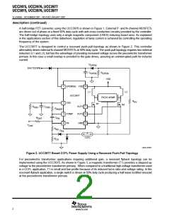
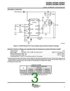
SLUS499A – NOVEMBER 2001 – REVISED JANUARY 2002
Terminal Functions
TERMINAL
NO.
UCCx975
UCCx976
UCCx977
I/O
DESCRIPTION
NAME
COMP
3
4
5
1
O
I
Output of the error amplifier and control voltage used to set the VCO frequency
Inverting input to the error amplifier
FB
GND
O
I
Ground reference for the device
OPEN/SD
Open lamp protection and a low power shut down
Common connection point for components that control the frequency range for the voltage con-
trolled oscillator (VCO)
OSC
2
7
I
Output of an internal CMOS driver used to drive an N-channel MOSFET (for UCC3977), or a
P-channel MOSFET (for UCC3976) left open for UCC3975
OUTP/OUT1
O
OUTN/OUT2
VDD
6
8
O
O
Output of an internal CMOS driver used to drive an N-channel MOSFET.
Connects to the battery or system voltage
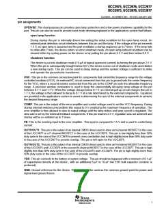
UCC2975, UCC2976
UCC3975, UCC3976
PW PACKAGE
UCC2977, UCC3977
PW PACKAGE
(TOP VIEW)
(TOP VIEW)
1
2
3
4
8
7
6
5
1
8
7
6
5
OPEN/SD
OSC
VDD
OPEN/SD
OSC
VDD
2
3
4
OUT1
OUT2
GND
OUTP
OUTN
GND
COMP
FB
COMP
FB
6
www.ti.com

 TI [ TEXAS INSTRUMENTS ]