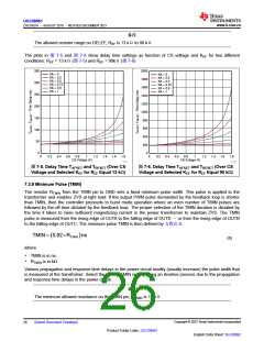
UCC28951
www.ti.com.cn
ZHCSIQ7A –AUGUST 2018 –REVISED DECEMBER 2021
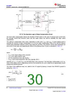
COMP
4
+
Oscillator
0.85 V
VREF VCM
CLK
PCM
Ramp
Generator
VMC
RAMP
Cycle-by-Cycle ILIM
RSUM
Two Direction
Current Sense
Ramp
Summing
CS_SLOPECOMP
11
+
+
-
CS 15
2 V
Mode Select
GND PCM
7
GND
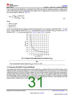
图7-9. The Operation Logic of Slope Compensation Circuit
Too much slope compensation reduces the benefits of PCM control. In the case of cycle-by-cycle current limit,
the average current limit becomes lower and this might reduce the start-up capability into large output
capacitances.
The optimum compensation ramp varies, depending on duty cycle, LOUT and LMAG. A good starting point in
selecting the amount of slope compensation is to set the slope compensation ramp to be half the inductor
current ramp downslope (inductor current ramp during the off time). The inductor current ramp downslope (as
seen at the CS pin input, and neglecting the effects of any filtering at the CS pin) is calculated in 方程式12:
V
L
R
OUT
CS
a1 × CT
m =
×
(12)
o
OUT
RAT
where
• VOUT is the output voltage of the converter
• LOUT is the output inductor value
• a1 is the transformer turns ratio (NP/NS)
• CTRAT is the current transformer ratio (IP/IS, typically 100:1)
Selection of LOUT, a1 and CTRAT are described later in this document. The total slope compensation is 0.5 m0.
Some of this ramp is due to magnetizing current in the transformer, the rest is added by an appropriately chosen
resistor from RSUM to ground.
The slope of the additional ramp, me, added to the CS signal by placing a resistor from RSUM to ground is
defined by 方程式13.
æ
ç
è
ö
÷
2.5
V
me =
0.5´RSUM ms
ø
(13)
where
• RSUM is in kΩ
• me is in V/μs
Copyright © 2023 Texas Instruments Incorporated
English Data Sheet: SLUSDB2
30
Submit Document Feedback
Product Folder Links: UCC28951

 TI [ TEXAS INSTRUMENTS ]