UCC28951
www.ti.com.cn
ZHCSIQ7A –AUGUST 2018 –REVISED DECEMBER 2021
备注
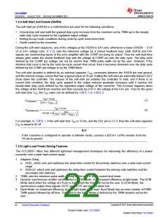
The allowed resistor range on DELEF, REF is 13 kΩto 90 kΩ.
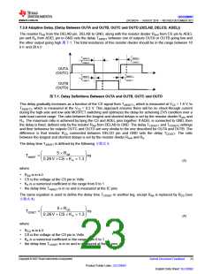
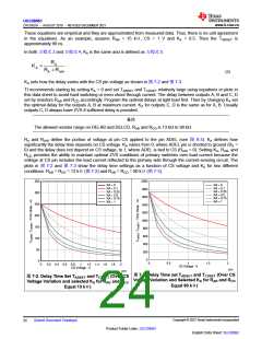
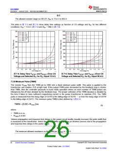
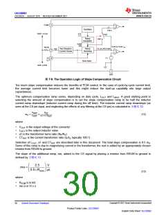
The plots in 图 7-5 and 图 7-6 show delay time settings as function of CS voltage and KEF for two different
conditions: REF = 13 kΩ(图7-5) and REF = 90kΩ(图7-6)
350
300
250
200
150
100
50
2000
1800
1600
1400
1200
1000
800
KA = 0
KA = 0
KA = 2.5
KA = 0.5
KA = 0.75
KA = 0.9
KA = 1
KA = 2.5
KA = 0.5
KA = 0.75
KA = 0.9
KA = 1
600
400
200
0
0
0
0.2
0.4
0.6
0.8
CS Voltage (V)
1
1.2
1.4
1.6
1.8
0
0.2
0.4
0.6
0.8
CS Voltage (V)
1
1.2
1.4
1.6
1.8
D007
D008
图7-5. Delay Time TAFSET and TBESET (Over CS
Voltage and Selected KEF for REF Equal 13 kΩ)
图7-6. Delay Time TAFSET and TBESET (Over CS
Voltage and Selected KEF for REF Equal 90 kΩ)
7.3.8 Minimum Pulse (TMIN)
The resistor RTMIN from the TMIN pin to GND sets a fixed minimum pulse width. This pulse is applied to the
transformer and enables ZVS at light load. If the output PWM pulse demanded by the feedback loop is shorter
than TMIN, then the controller proceeds to burst mode operation where an even number of TMIN pulses are
followed by the off time dictated by the feedback loop. The proper selection of the TMIN duration is dictated by
the time it takes to raise sufficient magnetizing current in the power transformer to maintain ZVS. The TMIN
pulse is measured from the rising edge of OUTA to the falling edge of OUTD – or from the rising edge of OUTB
to the falling edge of OUTC. The minimum pulse TMIN is then defined by 方程式8.
TMIN = 5.92´R
(
ns
)
TMIN
(8)
where
• TMIN is in ns
• RTMIN is in kΩ
Various propagation and response time delays in the power circuit modify (usually increase) the pulse width that
is measured at the transformer. Select the correct TMIN setting using an iterative process due to the propagation
and response time delays in the power circuit.
备注
The minimum allowed resistance on the TMIN pin, RTMIN is 10 kΩ.
Copyright © 2023 Texas Instruments Incorporated
English Data Sheet: SLUSDB2
26
Submit Document Feedback
Product Folder Links: UCC28951

 TI [ TEXAS INSTRUMENTS ]