UCC28951
www.ti.com.cn
ZHCSIQ7A –AUGUST 2018 –REVISED DECEMBER 2021
PWM
DCM Threshold
+ Hysteresis
CS
E
F
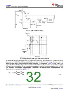
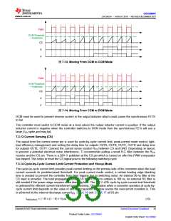
图7-13. Moving From DCM to CCM Mode
PWM
DCM Threshold
+ Hysteresis
CS
E
F
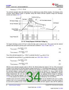
图7-14. Moving From CCM to DCM Mode
DCM must be used to prevent reverse current in the output inductor which could cause the synchronous FETS
to fail.
The controller must switch to DCM mode at a level where the output inductor current is positive. If the output
inductor current is negative when the controller switches to DCM mode then the synchronous FETs will see a
large VDS spike and may fail.
7.3.13 Current Sensing (CS)
The signal from the current sense pin is used for cycle-by-cycle current limit, peak-current mode control, light-
load efficiency management and setting the delay time for outputs OUTA, OUTB, OUTC, OUTD and delay time
for outputs OUTE, OUTF. Connect the current sense resistor RCS between CS and GND. Depending on layout,
to prevent a potential electrical noise interference, TI recommends pulling a small R-C filter between the RCS
resistor and the CS pin. There is a 200-Ω pulldown at the CS pin which is turned on after the PWM comparator
has tripped. This helps to reset the CS signal prior to the following switching cycle.
7.3.14 Cycle-by-Cycle Current Limit Current Protection and Hiccup Mode
The cycle-by-cycle current limit provides peak current limiting on the primary side of the converter when the load
current exceeds its predetermined threshold. For peak current mode control, a certain leading edge blanking
time is needed to prevent the controller from false tripping due to switching noise. An internal 30-ns filter at the
CS input is provided. The total propagation delay TCS from CS pin to outputs is 100 ns. An external RC filter is
still needed if the power stage requires more blanking time. The 2.0-V ±3% cycle-by-cycle current limit threshold
is optimized for efficient current transformer based sensing. The duration when a converter operates at cycle-by-
cycle current limit depends on the value of soft-start capacitor and how severe the overcurrent condition is. This
is achieved by the internal discharge current IDS 方程式16 and 方程式17 at SS pin.
I
= −25 × 1 − D + 5 µA
(16)
DS leader
Copyright © 2023 Texas Instruments Incorporated
Submit Document Feedback
33
Product Folder Links: UCC28951
English Data Sheet: SLUSDB2

 TI [ TEXAS INSTRUMENTS ]