UCC28951
www.ti.com.cn
ZHCSIQ7A –AUGUST 2018 –REVISED DECEMBER 2021
These equations are empirical and they are approximated from measured data. Thus, there is no unit agreement
in the equations. As an example, assume RAB = 15 kΩ, CS = 1 V and KA = 0.5. Then the TABSET is
approximately 90 ns.
In both 方程式3 and 方程式4, KA is the same and is defined as 方程式5:
RA
KA =
RA + RAHI
(5)
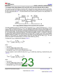
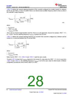
KA sets how the delay varies with the CS pin voltage as shown in 图7-2 and 图7-3.
TI recommends starting by setting KA = 0 and set TABSET and TCDSET relatively large using equations or plots in
this data sheet to avoid hard switching or even shoot through current. The delay between outputs A, B and C, D
set by resistors RAB and RCD accordingly. Program the optimal delays at light load first. Then by changing KA set
the optimal delay for the outputs A, B at maximum current. KA for outputs C, D is the same as for A, B. Usually
outputs C, D always have ZVS if sufficient delay is provided.
备注
The allowed resistor range on DELAB and DELCD, RAB and RCD is 13 kΩ to 90 kΩ.
RA and RAHI define the portion of voltage at pin CS applied to the pin ADEL (see 图 8-3). KA defines how
significantly the delay time depends on CS voltage. KA varies from 0, where ADEL pin is shorted to ground (RA =
0) and the delay does not depend on CS voltage, to 1, where ADEL is tied to CS (RAHI = 0). Setting KA, RAB, and
RCD provides the ability to maintain optimal ZVS conditions of primary switches over load current because the
voltage at CS pin includes the load current reflected to the primary side through the current-sensing circuit. The
plots in 图 7-2 and 图 7-3 show the delay time settings as a function of CS voltage and KA for two different
conditions: RAB = RCD = 13 kΩ(图7-2) and RAB = RCD = 90 kΩ(图7-3).
350
300
250
200
150
100
50
2000
1800
1600
1400
1200
1000
800
KA = 0
KA = 0
KA = 0.1
KA = 0.25
KA = 0.5
KA = 0.75
KA = 1
KA = 0.1
KA = 0.25
KA = 0.5
KA = 0.75
KA = 1
600
400
200
0
0
0
0.5
1
CS Voltage - V
1.5
2
0
0.2 0.4 0.6 0.8
1
CS Voltage - V
1.2 1.4 1.6 1.8
2
G001
G001
图7-3. Delay Time set TABSET and TCDSET (Over CS
Voltage Variation and Selected KA for RAB and RCD
Equal 90 kΩ)
图7-2. Delay Time Set TABSET and TCDSET (Over CS
Voltage Variation and selected KA for RAB and RCD
Equal 13 kΩ)
Copyright © 2023 Texas Instruments Incorporated
24
Submit Document Feedback
Product Folder Links: UCC28951
English Data Sheet: SLUSDB2

 TI [ TEXAS INSTRUMENTS ]