UCC28951
www.ti.com.cn
ZHCSIQ7A –AUGUST 2018 –REVISED DECEMBER 2021
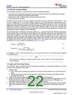
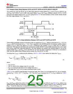
7.3.7 Adaptive Delay (Delay Between OUTA and OUTF, OUTB and OUTE (DELEF, ADELEF)
The resistor REF from the DELEF pin to GND along with the resistor divider RAEFHI from CS pin to ADELEF pin
and RAEF from ADELEF pin to GND sets equal delays TAFSET and TBESET between outputs OUTA or OUTB
going low and related output OUTF or OUTE going low 图 7-4. The total resistance of this resistor divider should
be in the range between 10 kΩand 20 kΩ.
OUTA
(OUTB)
OUTD
(OUTC)
TAFSET1
TBESET1
OUTF
(OUTE)
TAFSET2
TBESET2
图7-4. Delay Definitions Between OUTA and OUTF, OUTB and OUTE
These delays gradually increase as function of the CS signal from TAFSET1, which is measured at VCS = 0.2 V, to
TAFSET2, which is measured at VCS = 1.8 V. This is opposite to the DELAB and DELCD behavior and this delay is
longest (TAFSET2) when the signal at CS pin is maximized and shortest (TAFSET1) when the CS signal is
minimized. This approach will reduce the synchronous rectifier MOSFET body diode conduction time over a wide
load current range thus improving efficiency. The ratio between the longest and shortest delays is set by the
resistor divider RAEFHI and RAEF. If CS and ADELEF are tied, the ratio is maximized. If ADELEF is connected to
GND, then the delay is fixed, defined only by resistor REF from DELEF to GND.
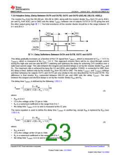
The delay time TAFSET is defined by the following 方程式6. 方程式6 also defines the delay time TBESET
.
æ
ö
æ
ç
è
ö
÷
ø
5´REF
TAFSET
=
ns + 4ns
ç
÷
ç
÷
2.65V - CS´KEF ´1.32
è
ø
(6)
where
• REF is in kΩ
• the CS, which is the voltage at pin CS, is in volts
• KEF is a numerical gain factor of CS voltage from 0 to 1
• the delay time TAFSET is in ns and is measured at the IC pins
方程式 6 is an empirical approximation of measured data, thus, there is no unit agreement in it. As an example,
assume REF = 15 kΩ, CS = 1 V and KEF = 0.5. Then the TAFSET is going to be 41.7 ns. KEF is defined as 方程式
7:
RAEF
KEF
=
RAEF + RAEF(hi)
(7)
RAEF and RAEFHI define the portion of voltage at pin CS applied to the pin ADELEF (see 图8-3). KEF defines how
significantly the delay time depends on CS voltage. KEF varies from 0, where ADELEF pin is shorted to ground
(RAEF = 0) and the delay does not depend on CS voltage, to 1, where ADELEF is tied to CS (RAEFHI = 0).
Copyright © 2023 Texas Instruments Incorporated
Submit Document Feedback
25
Product Folder Links: UCC28951
English Data Sheet: SLUSDB2

 TI [ TEXAS INSTRUMENTS ]