UCC28951
www.ti.com.cn
ZHCSIQ7A –AUGUST 2018 –REVISED DECEMBER 2021
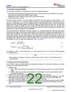
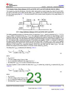
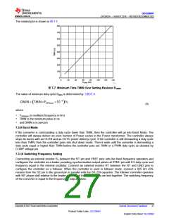
7.3.6 Adaptive Delay, (Delay Between OUTA and OUTB, OUTC and OUTD (DELAB, DELCD, ADEL))
The resistor RAB from the DELAB pin, DELAB to GND, along with the resistor divider RAHI from CS pin to ADEL
pin and RA from ADEL pin to GND sets the delay TABSET between one of outputs OUTA or OUTB going low and
the other output going high 图 7-1. The total resistance of this resistor divider should be in the range between 10
kΩand 20 kΩ
TABSET2
TCDSET2
TABSET2
TCDSET2
OUTA
(OUTC)
TABSET1
TCDSET1
TABSET1
TCDSET1
OUTB
(OUTD)
图7-1. Delay Definitions Between OUTA and OUTB, OUTC and OUTD
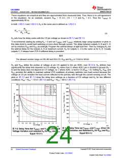
This delay gradually increases as a function of the CS signal from TABSET1, which is measured at VCS = 1.8 V, to
TABSET2, which is measured at the VCS = 0.2 V. This approach ensures there will be no shoot-through current
during the high-side and low-side MOSFET switching and optimizes the delay for acheiving ZVS condition over a
wide load current range. The ratio between the longest and shortest delays is set by the resistor divider RAHI and
RA. The maximum ratio is achieved by tying the CS and ADEL pins together. If ADEL is connected to GND, then
the delay is fixed, defined only by the resistor RAB from DELAB to GND. The delay TCDSET1 and TCDSET2 settings
and their behaviour for outputs OUTC and OUTD are very similar to the one described for OUTA and OUTB. The
difference is that resistor RCD connected between DELCD pin and GND sets the delay TCDSET. The ratio
between the longest and shortest delays is set by the resistor divider RAHI and RA.
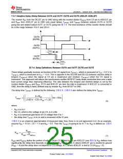
The delay time TABSET is defined by the following 方程式3.
æ
ç
è
ö
÷
ø
5 ´ RAB
TABSET
=
ns
0.26V + CS ´ KA ´ 1.3
(3)
where
• RAB is in kΩ
• CS is the voltage at the CS pin in Volts
• KA is a numerical coefficient in the range from 0 to 1
• the delay time TABSET is in ns and is measured at the IC pins
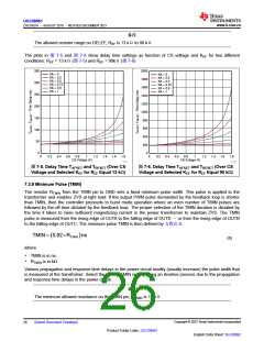
The same equation is used to define the delay time TCDSET in another leg, except RAB is replaced by RCD (see
方程式4).
æ
ç
è
ö
÷
ø
5 ´ RCD
TCDSET
=
ns
0.26V + CS ´ KA ´ 1.3
(4)
where
• RCD is in kΩ
• CS is the voltage at the CS pin in Volts
• KA is a numerical coefficient in the range from 0 to 1
• the delay time TCDSET is in ns and is measured at the IC pins
Copyright © 2023 Texas Instruments Incorporated
Submit Document Feedback
23
Product Folder Links: UCC28951
English Data Sheet: SLUSDB2

 TI [ TEXAS INSTRUMENTS ]