UCC27523, UCC27524, UCC27525, UCC27526
www.ti.com
SLUSAQ3F –NOVEMBER 2011–REVISED MAY 2013
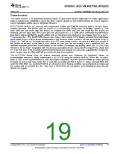
Drive Current and Power Dissipation
The UCC27523/4/5/6 family of drivers are capable of delivering 5-A of current to a MOSFET gate for a period of
several-hundred nanoseconds at VDD = 12 V. High peak current is required to turn the device ON quickly. Then,
to turn the device OFF, the driver is required to sink a similar amount of current to ground which repeats at the
operating frequency of the power device. The power dissipated in the gate driver device package depends on the
following factors:
•
Gate charge required of the power MOSFET (usually a function of the drive voltage VGS, which is very close
to input bias supply voltage VDD due to low VOH drop-out)
•
•
Switching frequency
Use of external gate resistors
Because UCC2752x features very low quiescent currents and internal logic to eliminate any shoot-through in the
output driver stage, their effect on the power dissipation within the gate driver can be safely assumed to be
negligible.
When a driver device is tested with a discrete, capacitive load calculating the power that is required from the bias
supply is fairly simple. The energy that must be transferred from the bias supply to charge the capacitor is given
by Equation 1.
1
2
EG
=
CLOADVDD
2
(1)
where is load capacitor and is bias voltage feeding the driver.
There is an equal amount of energy dissipated when the capacitor is charged. This leads to a total power loss
given by Equation 2.
2
LOAD DD SW
P
= C
V
f
G
where
•
fSW is the switching frequency
(2)
(3)
With VDD = 12 V, CLOAD = 10 nF and ƒSW = 300 kHz the power loss is calculated as (see Equation 3):
2
= 10nF´12V ´300kHz = 0.432W
P
G
Copyright © 2011–2013, Texas Instruments Incorporated
Submit Documentation Feedback
23
Product Folder Links: UCC27523, UCC27524, UCC27525, UCC27526

 TI [ TEXAS INSTRUMENTS ]