UCC27523, UCC27524, UCC27525, UCC27526
SLUSAQ3F –NOVEMBER 2011–REVISED MAY 2013
www.ti.com
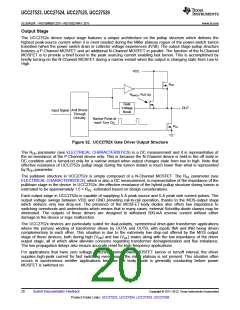
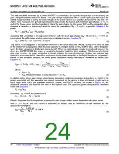
The switching load presented by a power MOSFET is converted to an equivalent capacitance by examining the
gate charge required to switch the device. This gate charge includes the effects of the input capacitance plus the
added charge needed to swing the drain voltage of the power device as it switches between the ON and OFF
states. Most manufacturers provide specifications that provide the typical and maximum gate charge, in nC, to
switch the device under specified conditions. Using the gate charge Qg, the power that must be dissipated when
charging a capacitor is determined which by using the equivalence Qg = CLOADVDD to provide Equation 4 for
power:
2
LOAD DD SW
P
= C
V
f
= Q V f
g DD SW
G
(4)
Assuming that UCC2752x is driving power MOSFET with 60 nC of gate charge (Qg = 60 nC at VDD = 12 V) on
each output, the gate charge related power loss is calculated as (see Equation 5):
P
= 2x60nC´12V ´300kHz = 0.432W
G
(5)
This power PG is dissipated in the resistive elements of the circuit when the MOSFET turns on or turns off. Half
of the total power is dissipated when the load capacitor is charged during turnon, and the other half is dissipated
when the load capacitor is discharged during turnoff. When no external gate resistor is employed between the
driver and MOSFET/IGBT, this power is completely dissipated inside the driver package. With the use of external
gate drive resistors, the power dissipation is shared between the internal resistance of driver and external gate
resistor in accordance to the ratio of the resistances (more power dissipated in the higher resistance component).
Based on this simplified analysis, the driver power dissipation during switching is calculated as follows (see
Equation 6):
æ
ç
è
ö
÷
ø
R
R
ON
OFF
P
= 0.5´Q ´ VDD´ f ´
SW
+
SW
G
R
+ R
R
+ R
ON GATE
OFF
GATE
where
•
•
ROFF = ROL
RON (effective resistance of pullup structure) = 1.5 x ROL
(6)
In addition to the above gate-charge related power dissipation, additional dissipation in the driver is related to the
power associated with the quiescent bias current consumed by the device to bias all internal circuits such as
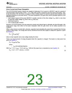
input stage (with pullup and pulldown resistors), enable, and UVLO sections. As shown in Figure 11, the
quiescent current is less than 0.6 mA even in the highest case. The quiescent power dissipation is calculated
easily with Equation 7.
P
= I
V
Q
DD DD
(7)
Assuming , IDD = 6 mA, the power loss is:
= 0.6 mA ´12V = 7.2mW
P
Q
(8)
Clearly, this power loss is insignificant compared to gate charge related power dissipation calculated earlier.
With a 12-V supply, the bias current is estimated as follows, with an additional 0.6-mA overhead for the
quiescent consumption:
P
0.432 W
G
I
~
=
= 0.036 A
DD
V
12 V
DD
(9)
24
Submit Documentation Feedback
Copyright © 2011–2013, Texas Instruments Incorporated
Product Folder Links: UCC27523, UCC27524, UCC27525, UCC27526

 TI [ TEXAS INSTRUMENTS ]