UCC27523, UCC27524, UCC27525, UCC27526
SLUSAQ3F –NOVEMBER 2011–REVISED MAY 2013
www.ti.com
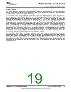
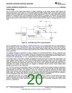
Output Stage
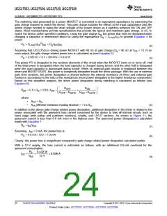
The UCC2752x device output stage features a unique architecture on the pullup structure which delivers the
highest peak-source current when it is most needed during the Miller plateau region of the power-switch turnon
transition (when the power switch drain or collector voltage experiences dV/dt). The output stage pullup structure
features a P-Channel MOSFET and an additional N-Channel MOSFET in parallel. The function of the N-Channel
MOSFET is to provide a brief boost in the peak sourcing current enabling fast turnon. This is accomplished by
briefly turning-on the N-Channel MOSFET during a narrow instant when the output is changing state from Low to
High.
VCC
ROH
RNMOS, Pull Up
Gate
Voltage
Boost
OUT
Anti Shoot-
Through
Circuitry
Input Signal
Narrow Pulse at
each Turn On
ROL
Figure 32. UCC2752X Gate Driver Output Structure
The ROH parameter (see ELECTRICAL CHARACTERISTICS) is a DC measurement and it is representative of
the on-resistance of the P-Channel device only. This is because the N-Channel device is held in the off state in
DC condition and is turned-on only for a narrow instant when output changes state from low to high. Note that
effective resistance of UCC2752x pullup stage during the turnon instant is much lower than what is represented
by ROH parameter.
The pulldown structure in UCC2752x is simply composed of a N-Channel MOSFET. The ROL parameter (see
ELECTRICAL CHARACTERISTICS), which is also a DC measurement, is representative of the impedance of the
pulldown stage in the device. In UCC2752x, the effective resistance of the hybrid pullup structure during turnon is
estimated to be approximately 1.5 × ROL, estimated based on design considerations.
Each output stage in UCC2752x is capable of supplying 5-A peak source and 5-A peak sink current pulses. The
output voltage swings between VDD and GND providing rail-to-rail operation, thanks to the MOS-output stage
which delivers very low drop-out. The presence of the MOSFET-body diodes also offers low impedance to
switching overshoots and undershoots which means that in many cases, external Schottky-diode clamps may be
eliminated. The outputs of these drivers are designed to withstand 500-mA reverse current without either
damage to the device or logic malfunction.
The UCC2752x devices are particularly suited for dual-polarity, symmetrical drive-gate transformer applications
where the primary winding of transformer driven by OUTA and OUTB, with inputs INA and INB being driven
complementary to each other. This situation is due to the extremely low drop-out offered by the MOS output
stage of these devices, both during high (VOH) and low (VOL) states along with the low impedance of the driver
output stage, all of which allow alleviate concerns regarding transformer demagnetization and flux imbalance.
The low propagation delays also ensure accurate reset for high-frequency applications.
For applications that have zero voltage switching during power MOSFET turnon or turnoff interval, the driver
supplies high-peak current for fast switching even though the miller plateau is not present. This situation often
occurs in synchronous rectifier applications because the body diode is generally conducting before power
MOSFET is switched on.
20
Submit Documentation Feedback
Copyright © 2011–2013, Texas Instruments Incorporated
Product Folder Links: UCC27523, UCC27524, UCC27525, UCC27526

 TI [ TEXAS INSTRUMENTS ]