UCC27523, UCC27524, UCC27525, UCC27526
www.ti.com
SLUSAQ3F –NOVEMBER 2011–REVISED MAY 2013
REVISION HISTORY
Changes from Original (November 2011) to Revision A
Page
•
Changed datasheet status to Production Data. .................................................................................................................... 1
Changes from Revision A (November 2011) to Revision B
Page
•
•
•
Added note to packaging section, "DSD package is rated MSL level 2". ............................................................................. 2
Changed Supply start threshold row to include two temperature ranges. ............................................................................ 5
Changed Minimum operating voltage after supply start min and max values from 3.6 V to 4.2 V to 3.40 V and 4.40
V. ........................................................................................................................................................................................... 5
•
•
•
Changed Supply voltage hysteresis typ value from 0.35 to 0.30. ........................................................................................ 5
Changed UCC27526 Block Diagram drawing. ................................................................................................................... 10
Changed UCC27526 Channel A in Inverting and Channel B in Non-Inverting Configuration drawing. ............................. 15
Changes from Revision B ( December 2011) to Revision C
Page
•
•
•
•
•
•
•
Added ROH note in the Outputs (OUTA, OUTB) section. ...................................................................................................... 5
Added an updated Output Stage section. ........................................................................................................................... 20
Added UCC2752X Gate Driver Output Structure image .................................................................................................... 20
Added an updated Low Propagation Delays and Tightly Matched Outputs section. ......................................................... 21
Added Slow Input Signal Combined with Differences in Input Threshold Voltage image. ................................................. 21
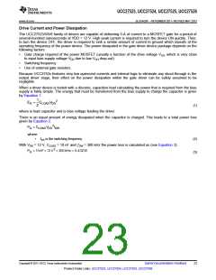
Added updated Drive Current and Power Dissipation section. ........................................................................................... 23
Added a PSW... equation. .................................................................................................................................................. 24
Changes from Revision C (March 2012) to Revision D
Page
•
•
•
•
Changed Inputs (INA, INB, INA+, INA-, INB+, INB-) section to include UCC2752X (D, DGN, DSD) information. .............. 5
Added Inputs (INA, INB, INA+, INA-, INB+, INB-) UCC27524P ONLY section. ................................................................... 5
Changed Enable (ENA, ENB) section to include UCC2752X (D, DGN, DSD) information. ................................................. 5
Added ENABLE (ENA, ENB) UCC27524P ONLY section. .................................................................................................. 5
Changes from Revision D (April 2012) to Revision E
Page
•
•
Added OUTA, OUTB voltage field and values. ..................................................................................................................... 3
Changed table note from "Values are verified by characterization and are not production tested." to "Values are
verified by characterization on bench." ................................................................................................................................. 3
•
•
•
•
Added note, "Values are verified by characterization and are not production tested." ........................................................ 3
Changed Switching Time tPW values from 10 ns and 25 ns to 15 ns and 25 ns ns. ............................................................ 5
Changed Functional Block Diagrams images. ...................................................................................................................... 9
Changed Slow Input Signal Figure 33. ............................................................................................................................... 21
Changes from Revision E (June 2012) to Revision F
Page
•
Added 0.5 to PSW equation in Drive Current and Power Dissipation section ..................................................................... 24
Copyright © 2011–2013, Texas Instruments Incorporated
Submit Documentation Feedback
27
Product Folder Links: UCC27523, UCC27524, UCC27525, UCC27526

 TI [ TEXAS INSTRUMENTS ]