UCC27523, UCC27524, UCC27525, UCC27526
www.ti.com
SLUSAQ3F –NOVEMBER 2011–REVISED MAY 2013
Low Propagation Delays and Tightly Matched Outputs
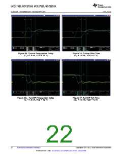
The UCC2752x driver devices feature a best in class, 13-ns (typical) propagation delay between input and output
which goes to offer the lowest level of pulse-transmission distortion available in the industry for high frequency
switching applications. For example in synchronous rectifier applications, the SR MOSFETs are driven with very
low distortion when a single driver device is used to drive both the SR MOSFETs. Further, the driver devices also
feature an extremely accurate, 1-ns (typ) matched internal-propagation delays between the two channels which
is beneficial for applications requiring dual gate drives with critical timing. For example in a PFC application, a
pair of paralleled MOSFETs may be driven independently using each output channel, which the inputs of both
channels are driven by a common control signal from the PFC controller device. In this case the 1ns delay
matching ensures that the paralleled MOSFETs are driven in a simultaneous fashion with the minimum of turnon
delay difference. Yet another benefit of the tight matching between the two channels is that the two channels are
connected together to effectively increase current drive capability, for example A and B channels may be
combined into a single driver by connecting the INA and INB inputs together and the OUTA and OUTB outputs
together. Then, a single signal controls the paralleled combination.
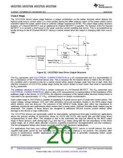
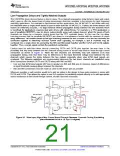
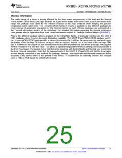
Caution must be exercised when directly connecting OUTA and OUTB pins together because there is the
possibility that any delay between the two channels during turnon or turnoff may result in shoot-through current
conduction as shown in Figure 33. While the two channels are inherently very well matched (4-ns Max
propagation delay), note that there may be differences in the input threshold voltage level between the two
channels which causes the delay between the two outputs especially when slow dV/dt input signals are
employed. The following guidelines are recommended whenever the two driver channels are paralleled using
direct connections between OUTA and OUTB along with INA and INB:
•
Use very fast dV/dt input signals (20 V/µs or greater) on INA and INB pins to minimize impact of differences
in input thresholds causing delays between the channels.
•
INA and INB connections must be made as close to the device pins as possible.
Wherever possible, a safe practice would be to add an option in the design to have gate resistors in series with
OUTA and OUTB. This allows the option to use 0-Ω resistors for paralleling outputs directly or to add appropriate
series resistances to limit shoot-through current, should it become necessary.
VDD
VDD
200 kW
200 kW
ENA
INA
1
2
8
7
ENB
ISHOOT-THROUGH
OUTA
VDD
Slow Input Signal
VIN_H
(Channel B)
VDD
400 kW
VIN_H
(Channel A)
VDD
VDD
UVLO
6
5
GND
INB
3
4
VDD
OUTB
400 kW
Figure 33. Slow Input Signal May Cause Shoot-Through Between Channels During Paralleling
(Recommended dV/dt Is 20 V/µs Or Higher)
Copyright © 2011–2013, Texas Instruments Incorporated
Submit Documentation Feedback
21
Product Folder Links: UCC27523, UCC27524, UCC27525, UCC27526

 TI [ TEXAS INSTRUMENTS ]