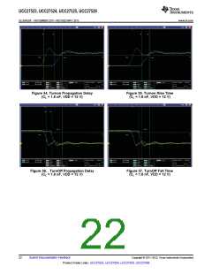
UCC27523, UCC27524, UCC27525, UCC27526
SLUSAQ3F –NOVEMBER 2011–REVISED MAY 2013
www.ti.com
PCB Layout
Proper PCB layout is extremely important in a high-current fast-switching circuit to provide appropriate device
operation and design robustness. The UCC27523/4/5/6 family of gate drivers incorporates short propagation
delays and powerful output stages capable of delivering large current peaks with very fast rise and fall times at
the gate of power MOSFET to facilitate voltage transitions very quickly. At higher VDD voltages, the peak current
capability is even higher (5-A peak current is at VDD = 12 V). Very high di/dt causes unacceptable ringing if the
trace lengths and impedances are not well controlled. The following circuit layout guidelines are strongly
recommended when designing with these high-speed drivers.
•
Locate the driver device as close as possible to power device in order to minimize the length of high-current
traces between the Output pins and the Gate of the power device.
•
Locate the VDD bypass capacitors between VDD and GND as close as possible to the driver with minimal
trace length to improve the noise filtering. These capacitors support high peak current being drawn from VDD
during turnon of power MOSFET. The use of low inductance SMD components such as chip resistors and
chip capacitors is highly recommended.
•
The turnon and turnoff current loop paths (driver device, power MOSFET and VDD bypass capacitor) should
be minimized as much as possible in order to keep the stray inductance to a minimum. High dI/dt is
established in these loops at 2 instances during turnon and turnoff transients, which will induce significant
voltage transients on the output pin of the driver device and Gate of the power MOSFET.
•
•
•
Wherever possible, parallel the source and return traces, taking advantage of flux cancellation
Separate power traces and signal traces, such as output and input signals.
Star-point grounding is a good way to minimize noise coupling from one current loop to another. The GND of
the driver is connected to the other circuit nodes such as source of power MOSFET and ground of PWM
controller at one, single point. The connected paths must be as short as possible to reduce inductance and
be as wide as possible to reduce resistance.
•
Use a ground plane to provide noise shielding. Fast rise and fall times at OUT may corrupt the input signals
during transition. The ground plane must not be a conduction path for any current loop. Instead the ground
plane must be connected to the star-point with one single trace to establish the ground potential. In addition
to noise shielding, the ground plane can help in power dissipation as well
•
•
In noisy environments, tiying inputs of an unused channel of UCC27526 to VDD (in case of INx+) or GND (in
case of INX-) using short traces in order to ensure that the output is enabled and to prevent noise from
causing malfunction in the output may be necessary.
Exercise caution when replacing the UCC2732x/UCC2742x devices with the UCC2752x:
–
–
UCC2752x is a much stronger gate driver (5-A peak current versus 4-A peak current).
UCC2752x is a much faster gate driver (13-ns/13-ns rise/fall propagation delay versus 25-ns/35-ns rise/fall
propagation delay).
26
Submit Documentation Feedback
Copyright © 2011–2013, Texas Instruments Incorporated
Product Folder Links: UCC27523, UCC27524, UCC27525, UCC27526

 TI [ TEXAS INSTRUMENTS ]