UCC27523, UCC27524, UCC27525, UCC27526
SLUSAQ3F –NOVEMBER 2011–REVISED MAY 2013
www.ti.com
Input Stage
The input pins of UCC2752x gate-driver devices are based on a TTL and CMOS compatible input-threshold logic
that is independent of the VDD supply voltage. With typically high threshold = 2.1 V and typically low threshold =
1.2 V, the logic level thresholds are conveniently driven with PWM control signals derived from 3.3-V and 5-V
digital power-controller devices. Wider hysteresis (typ 0.9 V) offers enhanced noise immunity compared to
traditional TTL logic implementations, where the hysteresis is typically less than 0.5 V. UCC2752x devices also
feature tight control of the input pin threshold voltage levels which eases system design considerations and
ensures stable operation across temperature (refer to Figure 14). The very low input capacitance on these pins
reduces loading and increases switching speed.
The UCC2752x devices feature an important safety feature wherein, whenever any of the input pins is in a
floating condition, the output of the respective channel is held in the low state. This is achieved using VDD pullup
resistors on all the Inverting inputs (INA, INB in UCC27523, INA in UCC27525 and INA-, INB- in UCC27526) or
GND pulldown resistors on all the non-inverting input pins (INA, INB in UCC27524, INB in UCC27525 and INA+,
INB+ in UCC27526), as shown in the device block diagrams.
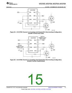
While UCC27523/4/5 devices feature one input pin per channel, the UCC27526 features a dual input
configuration with two input pins available to control the output state of each channel. With the UCC27526 device
the user has the flexibility to drive each channel using either a non-inverting input pin (INx+) or an inverting input
pin (INx-). The state of the output pin is dependent on the bias on both the INx+ and INx- pins (where x = A, B).
Once an Input pin is chosen to drive a channel, the other input pin of that channel (the unused input pin) must be
properly biased in order to enable the output of the channel. The unused input pin cannot remain in a floating
condition because, as mentioned earlier, whenever any input pin is left in a floating condition, the output of that
channel is disabled using the internal pullup or pulldown resistors for safety purposes. Alternatively, the unused
input pin is used effectively to implement an enable/disable function, as explained below.
•
•
•
In order to drive the channel x (x = A or B) in a non-inverting configuration, apply the PWM control input
signal to INx+ pin. In this case, the unused input pin, INx-, must be biased low (eg. tied to GND) in order to
enable the output of this channel.
–
Alternately, the INx- pin can be used to implement the enable/disable function using an external logic
signal. OUTx is disabled when INx- is biased High and OUTx is enabled when INX- is biased low.
In order to drive the channel x (x = A or B) in an Inverting configuration, apply the PWM control input signal to
INX- pin. In this case, the unused input pin, INX+, must be biased high (eg. tied to VDD) in order to enable
the output of the channel.
–
Alternately, the INX+ pin can be used to implement the enable/disable function using an external logic
signal. OUTX is disabled when INX+ is biased low and OUTX is enabled when INX+ is biased high.
Finally, it is worth noting that the UCC27526 output pin can be driven into high state only when INx+ pin is
biased high and INx- input is biased low.
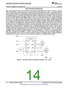
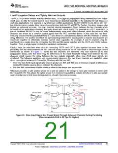
Refer to the input/output logic truth table and typical application diagram, (Figure 28 and Figure 29), for additional
clarification.
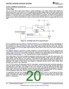
The input stage of each driver is driven by a signal with a short rise or fall time. This condition is satisfied in
typical power supply applications, where the input signals are provided by a PWM controller or logic gates with
fast transition times (<200 ns) with a slow changing input voltage, the output of the driver may switch repeatedly
at a high frequency. While the wide hysteresis offered in UCC2752x definitely alleviates this concern over most
other TTL input threshold devices, extra care is necessary in these implementations. If limiting the rise or fall
times to the power device is the primary goal, then an external resistance is highly recommended between the
output of the driver and the power device. This external resistor has the additional benefit of reducing part of the
gate-charge related power dissipation in the gate driver device package and transferring it into the external
resistor itself.
18
Submit Documentation Feedback
Copyright © 2011–2013, Texas Instruments Incorporated
Product Folder Links: UCC27523, UCC27524, UCC27525, UCC27526

 TI [ TEXAS INSTRUMENTS ]