UCC27523, UCC27524, UCC27525, UCC27526
www.ti.com
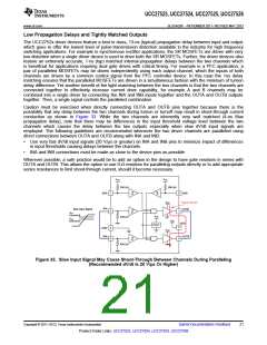
SLUSAQ3F –NOVEMBER 2011–REVISED MAY 2013
VDD and Under Voltage Lockout
The UCC2752x devices have internal undervoltage-lockout (UVLO) protection feature on the VDD pin supply
circuit blocks. When VDD is rising and the level is still below UVLO threshold, this circuit holds the output LOW,
regardless of the status of the inputs. The UVLO is typically 4.25 V with 350-mV typical hysteresis. This
hysteresis prevents chatter when low VDD supply voltages have noise from the power supply and also when
there are droops in the VDD bias voltage when the system commences switching and there is a sudden increase
in IDD. The capability to operate at low voltage levels such as below 5 V, along with best in class switching
characteristics, is especially suited for driving emerging GaN power semiconductor devices.
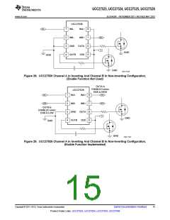
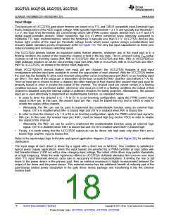
For example, at power up, the UCC2752x driver-device output remains LOW until the VDD voltage reaches the
UVLO threshold if Enable pin is active or floating. The magnitude of the OUT signal rises with VDD until steady-
state VDD is reached. The non-inverting operation in Figure 30 shows that the output remains LOW until the
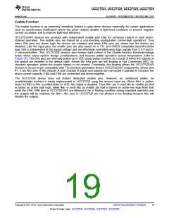
UVLO threshold is reached, and then the output is in-phase with the input. The inverting operation in Figure 31
shows that the output remains LOW until the UVLO threshold is reached, and then the output is out-phase with
the input. With UCC27526 the output turns to high-state only if INX+ is high and INX– is low after the UVLO
threshold is reached.
Because the device draws current from the VDD pin to bias all internal circuits, for the best high-speed circuit
performance, two VDD bypass capacitors are recommended to prevent noise problems. The use of surface
mount components is highly recommended. A 0.1-μF ceramic capacitor must be located as close as possible to
the VDD to GND pins of the gate-driver device. In addition, a larger capacitor (such as 1-μF) with relatively low
ESR must be connected in parallel and close proximity, in order to help deliver the high-current peaks required
by the load. The parallel combination of capacitors presents a low impedance characteristic for the expected
current levels and switching frequencies in the application.
VDD Threshold
VDD Threshold
VDD
EN
VDD
EN
IN
IN
OUT
OUT
UDG-11229
UDG-11228
Figure 30. Power-Up Non-Inverting Driver
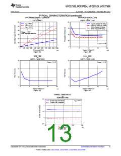
Operating Supply Current
Figure 31. Power-Up Inverting Driver
The UCC2752x products feature very low quiescent IDD currents. The typical operating-supply current in UVLO
state and fully-on state (under static and switching conditions) are summarized in Figure 10, Figure 11 and
Figure 12. The IDD current when the device is fully on and outputs are in a static state (DC high or DC low, refer
Figure 11) represents lowest quiescent IDD current when all the internal logic circuits of the device are fully
operational. The total supply current is the sum of the quiescent IDD current, the average IOUT current due to
switching and finally any current related to pullup resistors on the enable pins and inverting input pins. For
example when the inverting Input pins are pulled low additional current is drawn from VDD supply through the
pullup resistors (refer to Figure 6 though Figure 9). Knowing the operating frequency (fSW) and the MOSFET gate
(QG) charge at the drive voltage being used, the average IOUT current can be calculated as product of QG and
fSW
.
A complete characterization of the IDD current as a function of switching frequency at different VDD bias voltages
under 1.8-nF switching load in both channels is provided in Figure 22. The strikingly linear variation and close
correlation with theoretical value of average IOUT indicates negligible shoot-through inside the gate-driver device
attesting to its high-speed characteristics.
Copyright © 2011–2013, Texas Instruments Incorporated
Submit Documentation Feedback
17
Product Folder Links: UCC27523, UCC27524, UCC27525, UCC27526

 TI [ TEXAS INSTRUMENTS ]