UCC27523, UCC27524, UCC27525, UCC27526
SLUSAQ3F –NOVEMBER 2011–REVISED MAY 2013
www.ti.com
Introduction
The UCC2752x family of products represent Texas Instruments’ latest generation of dual-channel low-side high-
speed gate-driver devices featuring 5-A source/sink current capability, industry best-in-class switching
characteristics and a host of other features listed in Table 3 all of which combine to ensure efficient, robust and
reliable operation in high-frequency switching power circuits.
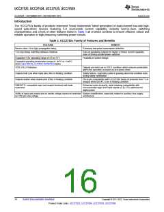
Table 3. UCC2752x Family of Features and Benefits
FEATURE
Best-in-class 13-ns (typ) propagation delay
1-ns (typ) delay matching between channels
BENEFIT
Extremely low-pulse transmission distortion
Ease of paralleling outputs for higher (2 times) current capability,
ease of driving parallel-power switches
Expanded VDD Operating range of 4.5 to 18 V
Flexibility in system design
Expanded operating temperature range of –40°C to +140°C
(See ELECTRICAL CHARACTERISTICS table)
VDD UVLO Protection
Outputs are held Low in UVLO condition, which ensures predictable,
glitch-free operation at power-up and power-down
Outputs held Low when input pins (INx) in floating condition
Outputs enable when enable pins (ENx) in floating condition
Safety feature, especially useful in passing abnormal condition tests
during safety certification
Pin-to-pin compatibility with UCC2732X family of products from TI, in
designs where pin #1, 8 are in floating condition
CMOS/TTL compatible input and enable threshold with wide
hysteresis
Enhanced noise immunity, while retaining compatibility with
microcontroller logic level input signals (3.3V, 5V) optimized for
digital power
Ability of input and enable pins to handle voltage levels not restricted System simplification, especially related to auxiliary bias supply
by VDD pin bias voltage architecture
16
Submit Documentation Feedback
Copyright © 2011–2013, Texas Instruments Incorporated
Product Folder Links: UCC27523, UCC27524, UCC27525, UCC27526

 TI [ TEXAS INSTRUMENTS ]