UCC21759-Q1
SLUSEB4A – AUGUST 2020 – REVISED DECEMBER 2020
www.ti.com
11 Layout
11.1 Layout Guidelines
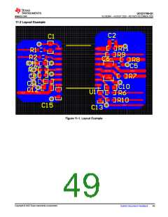
Due to the strong drive strength of UCC21759-Q1, careful considerations must be taken in PCB design. Below
are some key points:
•
The driver should be placed as close as possible to the power semiconductor to reduce the parasitic
inductance of the gate loop on the PCB traces
•
The decoupling capacitors of the input and output power supplies should be placed as close as possible to
the power supply pins. The peak current generated at each switching transient can cause high dI/dt and
voltage spike on the parasitic inductance of PCB traces
•
The driver COM pin should be connected to the Kelvin connection of SiC MOSFET source or IGBT emitter. If
the power device does not have a split Kelvin source or emitter, the COM pin should be connected as close
as possible to the source or emitter terminal of the power device package to separate the gate loop from the
high power switching loop
•
•
Use a ground plane on the input side to shield the input signals. The input signals can be distorted by the
high frequency noise generated by the output side switching transients. The ground plane provides a low-
inductance filter for the return current flow
If the gate driver is used for the low side switch which the COM pin connected to the dc bus negative, use the
ground plane on the output side to shield the output signals from the noise generated by the switch node; if
the gate driver is used for the high side switch, which the COM pin is connected to the switch node, ground
plane is not recommended
•
•
If ground plane is not used on the output side, separate the return path of the DESAT and AIN ground loop
from the gate loop ground which has large peak source and sink current
No PCB trace or copper is allowed under the gate driver. A PCB cutout is recommended to avoid any noise
coupling between the input and output side which can contaminate the isolation barrier
Copyright © 2020 Texas Instruments Incorporated
48
Submit Document Feedback

 TI [ TEXAS INSTRUMENTS ]