UCC21759-Q1
SLUSEB4A – AUGUST 2020 – REVISED DECEMBER 2020
www.ti.com
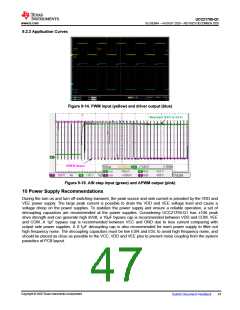
9.2.3 Application Curves
Figure 9-14. PWM input (yellow) and driver output (blue)
Step Input (0.6 V to 4.5 V)
APWM Output
Figure 9-15. AIN step input (green) and APWM output (pink)
10 Power Supply Recommendations
During the turn on and turn off switching transient, the peak source and sink current is provided by the VDD and
VEE power supply. The large peak current is possible to drain the VDD and VEE voltage level and cause a
voltage droop on the power supplies. To stabilize the power supply and ensure a reliable operation, a set of
decoupling capacitors are recommended at the power supplies. Considering UCC21759-Q1 has ±10A peak
drive strength and can generate high dV/dt, a 10µF bypass cap is recommended between VDD and COM, VEE
and COM. A 1µF bypass cap is recommended between VCC and GND due to less current comparing with
output side power supplies. A 0.1µF decoupling cap is also recommended for each power supply to filter out
high frequency noise. The decoupling capacitors must be low ESR and ESL to avoid high frequency noise, and
should be placed as close as possible to the VCC, VDD and VEE pins to prevent noise coupling from the system
parasitics of PCB layout.
Copyright © 2020 Texas Instruments Incorporated
Submit Document Feedback
47

 TI [ TEXAS INSTRUMENTS ]